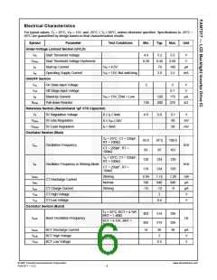
Electrical Characteristics (Continued)
For typical values, TA = 25°C, VIN = 15V, and -25°C ≤ TA ≤ 85°C, unless otherwise specified. Specifications to -25°C ~
85°C are guaranteed by design based on final characterization results.
Symbol
Parameter
Test Conditions
Min.
Typ.
Max.
Unit
Error Amplifier Section
AV
Gm
lsin
Open-loop Gain(3)
37
40
dB
µmho
µA
Error Amplifier Trans-conductance
Output Sink Current
20
-50
12
60
-20
32
OLP = 2.25V
-35
22
lsur
Output Source Current
OLP = 0.8V
µA
Ibsin
Burst CMP Sink Current
38
52
66
µA
TA = 25°C
1.275
1.255
-1
1.350
1.350
0
1.421
1.444
1
V135p
1.35V Regulation Voltage
V
Iolpi
Iolpo
Volpr
OLP Input Current
OLP = 2V
OLP = -2V
µA
µA
V
OLP Output Current
OLP Input Voltage Range(3)
-30
-4
-20
-10
4
Open-Lamp Regulation Section
Striking, OLR =
Iolr1
-2.0
-1.0
-0.1
µA
Error Amplifier Source Current for
Open-Lamp Regulation
Volr1+0.05
Iolr2
Volr1
Volr2
Volr3
OLR = 2.1V
Striking
0
µA
V
Open-Lamp Regulation Voltage 1
Open-Lamp Regulation Voltage 2
Open-Lamp Regulation Voltage 3
1.65
1.95
2.1
1.80
2.05
2.2
1.95
2.15
2.3
Striking
V
V
OLR Error Amplifier Trans-
conductance
GmOLR
200
350
500
µmho
Iolrsi
Iolri
OLR Error Amplifier Sink Current
OLR Input Current
Normal, OLR = 2.5V
OLR = 1.5V
50
10
-25
-4
70
17
90
24
-7
4
µA
µA
µA
V
Iolro
Volrr
OLR Output Current
OLR Input Voltage Range(3)
OLR = -1.5V
-15
Note:
3. These parameters, although guaranteed, are not 100% tested in production.
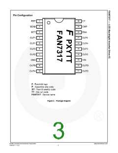
© 2007 Fairchild Semiconductor Corporation
www.fairchildsemi.com
FAN7317 • 1.0.2
7

 FAIRCHILD [ FAIRCHILD SEMICONDUCTOR ]