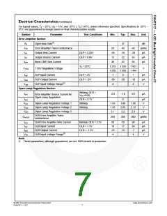
Electrical Characteristics (Continued)
For typical values, TA = 25°C, VIN = 15V, and -25°C ≤ TA ≤ 85°C, unless otherwise specified. Specifications to -25°C ~
85°C are guaranteed by design based on final characterization results.
Protection Section
Volp0
Volp1
Vcmpr
Varcp
Vhfbp
Vslp
Open-Lamp Protection Voltage 0(4)
Open-Lamp Protection Voltage 1
CMP-High Protection Voltage
Arc Protection Voltage
Open Lamp in Striking
Open Lamp
0.95
0.44
2.95
2.90
3.4
1.00
0.51
3.05
3.05
3.5
1.05
0.58
3.15
3.20
3.6
V
V
V
V
High-FB Protection Voltage(4)
V
Short Lamp Protection Voltage
0.24
0.32
1.6
0.40
V
Tolps
Tolpn
Tcmprs
Tcmprn
Tolr
Striking, foscb = 330Hz
Normal, fosc = 100kHz
Striking, foscb = 330Hz
Normal, fosc = 100kHz
Normal, fosc = 100kHz
Normal, fosc = 100kHz
s
Open-Lamp Protection Delay(4)
High-CMP Protection Delay(4)
10
ms
s
1.6
10
ms
µs
ms
°C
Open-Lamp Regulation Delay(4)
Short Lamp Protection Delay(4)
Thermal Shutdown(4)
320
1
Tslp
TSD
150
Output Section
Vpdhv
Vphlv
Vndhv
Vndlv
PMOS Gate High Voltage(4)
VIN = 15V
VIN = 15V
VIN = 15V
VIN = 15V
VIN
VIN-7
7.0
0
V
V
V
V
PMOS Gate Low Voltage
NMOS Gate High Voltage
NMOS Gate Low Voltage(4)
VIN-6.5
6.5
VIN-7.5
7.5
PMOS Gate Voltage with UVLO
Activated
NMOS Gate Voltage with UVLO
Activated
Vpuv
Vnuv
VIN = 4.5V
VIN = 4.5V
VIN-0.3
V
V
0.3
Ipdsur
Ipdsin
Indsur
Indsin
tr
PMOS Gate Drive Source Current(4)
PMOS Gate Drive Sink Current(4)
NMOS Gate Drive Source Current(4)
NMOS Gate Drive Sink Current(4)
Rising Time(4)
VIN = 15V
-200
300
200
-300
70
mA
mA
mA
mA
ns
VIN = 15V
VIN = 15V
VIN = 15V
VIN = 15V, Cload = 2nF
VIN = 15V, Cload = 2nF
tf
Falling Time(4)
70
ns
Maximum / Minimum Overlap
Minimum Overlap Between Diagonal
fosc = 100kHz
fosc = 100kHz
0
%
%
Switches(4)
Maximum Overlap Between Diagonal
86
90
Switches(4)
Dead Time
Note:
PDR_A/NDR_B(4)
PDR_C/NDR_D(4)
150
150
200
200
250
250
ns
ns
4. These Parameters, although guaranteed, are not 100% tested in production.
© 2007 Fairchild Semiconductor Corporation
www.fairchildsemi.com
FAN7317 • 1.0.2
8

 FAIRCHILD [ FAIRCHILD SEMICONDUCTOR ]