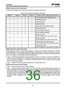
ST16C650A
2.90V TO 5.5V UART WITH 32-BYTE FIFO
áç
REV. 5.0.0
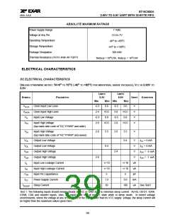
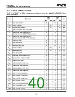
AC ELECTRICAL CHARACTERISTICS
TA=0O TO 70OC (-40O TO +85OC FOR INDUSTRIAL GRADE PACKAGE), VCC IS 2.90V TO 5.5V, 70 PF LOAD
WHERE APPLICABLE
LIMITS
3.3V
LIMITS
5.0V
SYMBOL
PARAMETER
UNIT
MIN
MAX MIN
MAX
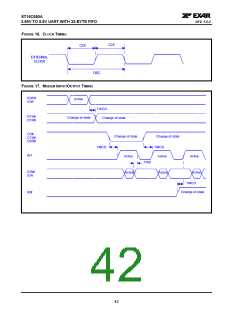
CLK
OSC
OSC
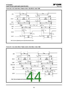
TAS
Clock Pulse Duration
Crystal Frequency
30
20
ns
MHz
MHz
ns
20
33
24
50
External Clock Frequency
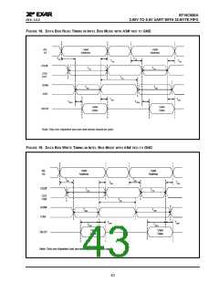
Address Setup Time (AS# tied to GND)
5
5
Address Hold Time (AS# tied to GND)
10
10
ns
TAH
(top mark date code of "HC YYWW" and older)
Address Hold Time (AS# tied to GND)
0
0
ns
TAH
(top mark date code of "I2 YYWW" and newer)
Chip Select Width
50
50
40
40
40
30
ns
ns
ns
ns
ns
ns
ns
ns
ns
ns
ns
ns
ns
ns
ns
ns
ns
ns
ns
ns
TCS
TRD
IOR# Strobe Width
TDY
Read/Write Cycle Delay
TRDV
TDD
Data Access Time
40
15
30
10
Data Disable Time
0
50
20
5
0
40
10
5
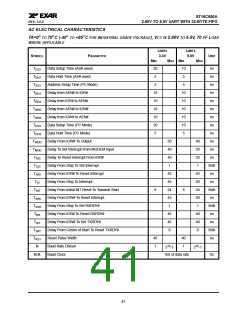
TWR
TDS1
TDH1
TASW
TAS1
TAH1
TAS2
TAH2
TCS1
TCSH
TCS2
TRD1
TRD2
TDIS
TWR1
IOW# Strobe Width
Data Setup Time (AS# tied to GND)
Data Hold Time (AS# tied to GND)
Address Strobe Width
35
5
25
5
Address Setup Time (AS# used)
Address Hold Time (AS# used)
Address Setup Time (AS# used)
Address Hold Time (AS# used)
Delay from Chip Select to AS#
Delay from AS# to Chip Select
Delay from AS# to Chip Select
Delay from AS# to Read
10
5
10
5
10
5
10
5
0
0
5
5
10
10
15
10
10
10
10
10
Delay from Chip Select to IOR#
Delay from IOR# to DDIS#
Delay from AS# to IOW#
40

 EXAR [ EXAR CORPORATION ]