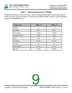
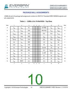
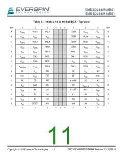
EMD3D256M08BS1
EMD3D256M16BS1
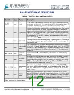
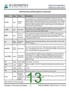
Ball Functions and Descriptions (Continued)
Symbol
Type
Name
Description
Auto-precharge: A10 is sampled during READ/WRITE commands to determine
whether Autoprecharge should be performed to the accessed bank after the READ/
WRITE operation. (HIGH: Autoprecharge; LOW: no Autoprecharge). A10 is sampled
during a Precharge command to determine whether the Precharge applies to one
bank (A10 LOW) or all banks (A10 HIGH). If only one bank is to be precharged, the
bank is selected by bank addresses.
Auto Pre-
charge
A10/AP
Input
Burst Chop: A12 / BC is sampled during READ and WRITE commands to determine
if burst chop (on-the-fly) will be performed. (HIGH, no burst chop; LOW: burst
chopped). See command truth table for details.
A12/BC
RESET
Input
Burst Chop
Active Low Asynchronous Reset: Reset is active when RESET is LOW, and inactive
Acitve Low
Asynchro-
nous Reset
when RESET is HIGH. RESET must be HIGH during normal operation. RESET is a
CMOS rail-to-rail signal with DC high and low at 80% and 20% of VDD, i.e. 1.20V for
DC high and 0.30V for DC low.
Input
Input/
Output Output
Data Input/
Data Input/ Output: Bi-directional data bus. DQ0-7 (x8) and DQ8-15 (x16) are refer-
DQ
enced to V
.
REFDQ in
Data strobe: Output with read data. Edge-aligned with read data. Input with write
data. Center-aligned to write data. For x16 operation DQSL/DQSL is associated with
DQ0-7 and DQSU/DQSU is associated with DQ8-15.
Input/
DQS/DQS
Data Strobe
Output
Output
Termination data strobe: Applies to the x8 configuration only. When enabled via
Mode Register A11=1 in MR1, STT-MRAM will enable the same termination resis-
tance function on TDQS/TDQS that is applied to DQS/DQS. When disabled via
mode register A11=0 in MR1, DM/TDQS will provide the data mask function and
TDQS is not used.
Termination
Data Strobe
TDQS, TDQS
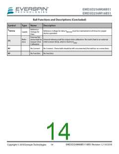
VDD
Supply
Supply
Supply
Supply
Power Supply Power supply: 1.5V 0.075V.
VDDQ
DQ Power
Supply
DQ power supply: 1.5V 0.075V. Isolated on the device for improved noise immu-
nity.
VSS
Ground
Ground
VSSQ
DQ Ground
DQ ground: Isolated on the device for improved noise immunity.
Reference
Voltage for
Control, Com-
mand and
Address
Reference voltage for control, command, and address: V
at all times for proper device operation.
must be maintained
REFCA
VREFCA
Supply
Table continues on the next page.
EMD3D256M08BS1/16BS1 Revision 1.3 10/2018
Copyright © 2018 Everspin Technologies
13

 EVERSPIN [ Everspin Technologies ]