EMD3D256M08BS1
EMD3D256M16BS1
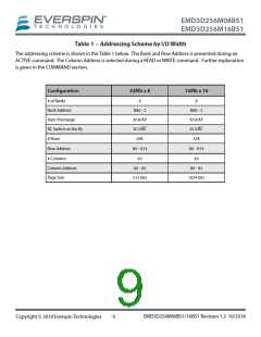
Table 1 – Addressing Scheme by I/O Width
The addressing scheme is shown in the Table 1 below. The Bank and Row Address is presented during an
ACTIVE command. The Column Address is selected during a READ or WRITE command. Further explanation
is given in the COMMAND section.
Configuration
# of Banks
32Mb x 8
8
16Mb x 16
8
Bank Address
Auto Precharge
BC Switch on the fly
# Rows
BA0 - 2
A10/AP
A12/BC
64K
BA0 - 2
A10/AP
A12/BC
32K
Row Address
# Columns
A0 - A15
64
A0 - A14
64
Column Address
Page Size
A0 - A5
512 bits
A0 - A5
1024 bits
EMD3D256M08BS1/16BS1 Revision 1.3 10/2018
Copyright © 2018 Everspin Technologies
9

 EVERSPIN [ Everspin Technologies ]