EMD3D256M08BS1
EMD3D256M16BS1
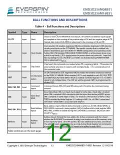
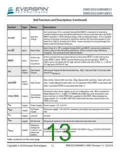
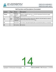
BALL FUNCTIONS AND DESCRIPTIONS
Table 4 – Ball Functions and Descriptions
Symbol
Type
Name
Description
Clock: CK and CK are differential clock inputs. All control and address input signals
are sampled on the crossing of the positive edge of CK and the negative edge of CK.
Output data strobe (DQS, DQS) is referenced to the crossings of CK and CK.
CK, CK
Input
Clock
Clock enable: CKE enables (registered HIGH) and disables (registered LOW) internal
circuitry and clocks on the STT-MRAM. The specific circuitry that is enabled/ dis-
abled is dependent upon the DDR3 STT-MRAM configuration and operating mode.
CKE
Input
Clock Enable Taking CKE LOW provides PRECHARGE POWER-DOWN, or active power-down (row
active in any bank). CKE is synchronous for power-down entry and exit. Input buf-
fers (excluding CK, CK, CKE, RESET, and ODT) are disabled during POWER-DOWN.
CKE is referenced to V
.
REFCA
Chip Select: All commands are masked when CS is registered HIGH. CS provides for
CS
Input
Input
Chip Select
external Rank selection on systems with multiple Ranks. CS is considered part of
the command code.
On Die Termination: ODT (registered HIGH) enables termination resistance internal
to the DDR3 STT-MRAM. When enabled, ODT is only applied to each DQ, DQS, DQS
and DM/TDQS, NU/TDQS (When TDQS is enabled via Mode Register A11=1 in MR1)
signal for x8 configurations. The ODT pin will be ignored if MR1 is programmed to
disable ODT.
On-Die Termi-
nation
ODT
Command
Inputs
Command Inputs: RAS, CAS and WE (along with CS) define the command being
entered.
RAS, CAS, WE Input
Input Data Mask: DM is an input mask signal for write data. Input data is masked
when DM is sampled HIGH coincident with that input data during a WRITE access.
DM is sampled on both edges of DQS. For x8 device, the function of DM or TDQS/
TDQS is enabled by Mode Register A11 setting in MR1. For x16 DML is associated
with DQ0-7 while DMU is associated with DQ8-15.
Input Data
Mask
DM
Input
Bank address inputs: BA[2:0] define the bank to which an ACTIVE, READ, WRITE, or
Bank Address PRECHARGE command is being applied. BA[2:0] define which mode register (MR0,
BA0, BA1, BA2 Input
Inputs
MR1, MR2, or MR3) is loaded during the LOAD MODE command. BA[2:0] are refer-
enced to V
.
REFCA
Address Inputs: Provide the row address for Active commands and the column
address for READ/WRITE commands to select one location out of the memory array
in the respective bank. (A10/AP and A12/BC have additional functions, see below).
The address inputs also provide the op-code during Mode Register Set commands.
In using the device in x16 mode A15 needs to be pulled to logic HIGH.
Address
Inputs
A0-A15
Input
Table continues on the next page.
EMD3D256M08BS1/16BS1 Revision 1.3 10/2018
Copyright © 2018 Everspin Technologies
12

 EVERSPIN [ Everspin Technologies ]