ZSPM1025A
True Digital PWM Controller (Single-Phase, Single-Rail)
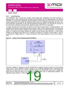
3.3.3.
Digital Compensator
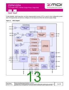
The sampled output voltage is processed by a digital control loop in order to modulate the DPWM output signals
controlling the power stage. This digital control loop works as a voltage-mode controller using a PID-type
compensation. The basic structure of the controller is shown in Figure 3.1. The proprietary State-Law™ Control
(SLC) concept features two parallel compensators, steady-state operation, and fast transient operation. The
ZSPM1025A implements fast, reliable switching between the different compensation modes in order to ensure
good transient performance and quiet steady state. This allows tuning the compensators individually for the
respective needs; i.e. quiet steady-state and fast transient performance.
Figure 3.1
Simplified Block Diagram of the Digital Compensation
Coefficients
Steady-state
Operation
Mode
Transient
Detection
Digital PID
Compensator
Non-linear
Gain
Digital Error Signal
Duty Cycle
Three additional techniques are used to improve transient performance further.
Tru-sample Technology™ is used to acquire fast, accurate, and continuous information about the output
voltage so that the device can react quickly to any change in output voltage. Tru-sample Technology™
reduces phase-lag caused by sampling delays, reduces noise sensitivity, and improves transient
performance.
The Sub-cycle Response™ (SCR) technique, a method to drive the DPWM asynchronously during load
transients, allows limiting the maximum deviation of the output voltage and recharging the output
capacitors faster.
A non-linear gain adjustment is used during large load transients to boost the loop gain and reduce the
settling time.
3.3.4.
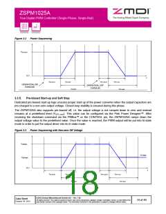
Power Sequencing and the CONTROL Pin
The ZSPM1025A supports power-sequencing features including programmable ramp up/down and delays. The
typical sequence of events is shown in Figure 3.2 and follows the PMBus™ standard. The individual values can
be set using the appropriate configuration setting, which can be selected using the Pink Power Designer™ GUI.
Three different configuration options are supported to turn the device on. The device can be configured to turn on
immediately after POR, on an OPERATION_ON command, or on an edge on the CONTROL pin.
© 2013 Zentrum Mikroelektronik Dresden AG — Rev. 1.00
All rights reserved. The material contained herein may not be reproduced, adapted, merged, translated, stored, or used without the
prior written consent of the copyright owner. The information furnished in this publication is subject to changes without notice.
Data Sheet
October 24, 2013
17 of 46

 ETC [ ETC ]