ZSPM1025A
True Digital PWM Controller (Single-Phase, Single-Rail)
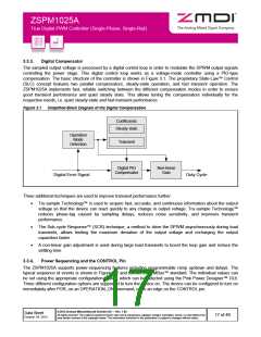
3.4.1.
Output Over/Under-Voltage
To prevent damage to the load, the ZSPM1025A utilizes an output over-voltage protection circuit. The voltage at
VFBP is continuously compared with a configurable fault threshold using a high-speed analog comparator. The
fault threshold can be configured using the Pink Power Designer™ GUI. If the voltage exceeds the configured
threshold, the fault response is generated and the PWM output is set to low impedance (clamped to PGND). The
voltage fault level is generated by a 6-bit DAC with a reference voltage of 1.60 V resulting in 25 mV resolution.
The output voltage is also sampled using the HKADC and continuously compared to a configurable output over-
voltage warning threshold. The warning threshold can be configured using the Pink Power Designer™ GUI. If the
output voltage exceeds this threshold, a warning is generated.
The ZSPM1025A also monitors the output voltage with two lower thresholds. If the output voltage is below the
under-voltage warning level and above the under-voltage fault level, an output voltage under-voltage warning is
triggered. If the output voltage falls below the fault level, a fault event is generated and the output is set to low
impedance.
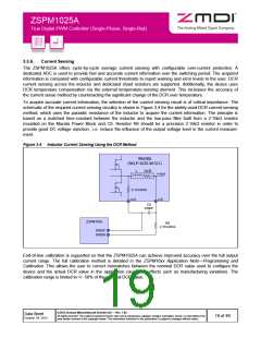
3.4.2.
Output Current Protection and Limiting
The ZSPM1025A continuously monitors the average inductor current and utilizes this information to protect the
power supply against excessive output current. The output over-current warning and fault threshold levels can be
configured using the Pink Power Designer™ GUI. If the fault level is exceeded, the PWM output is set to low
impedance.
3.4.3.
Over-Temperature Protection
The ZSPM1025A monitors internal and external temperature. For each, a warning and a fault level can be
configured and an appropriate response can be enabled.
3.5. Configuration
The ZSPM1025A incorporates two different sets of configuration parameters (see section 4.4). The first set of
configuration parameters can be configured during design time and cannot be changed during run-time. The
second set of configuration parameters can be configured during design time, but can also be reconfigured during
run-time using the appropriate PMBus™ command. Note that these reconfigured values are not stored in the OTP
memory, so they are lost during power cycling the device.
In order to evaluate the device and its configuration on the bench, a special engineering mode is supported by the
device and Pink Power Designer™. In this engineering mode, the device can be reconfigured multiple times
without writing the configuration into the OTP. During this mode, the device starts up after power-on reset in an
unconfigured state. The Pink Power Designer™ then provides the configuration to the ZSPM1025A, enabling full
operation without actually configuring the OTP. The engineer can use this mode to evaluate the configuration on
the bench. However, the configuration will be lost upon power-on-reset.
After the design engineer has determined the final configuration options, an OTP image can be created that is
then written into the ZSPM1025A. This can be either on the bench using the Pink Power Designer™ or in end–of-
line testing during mass production.
© 2013 Zentrum Mikroelektronik Dresden AG — Rev. 1.00
All rights reserved. The material contained herein may not be reproduced, adapted, merged, translated, stored, or used without the
prior written consent of the copyright owner. The information furnished in this publication is subject to changes without notice.
Data Sheet
October 24, 2013
21 of 46

 ETC [ ETC ]