ZSPM1025A
True Digital PWM Controller (Single-Phase, Single-Rail)
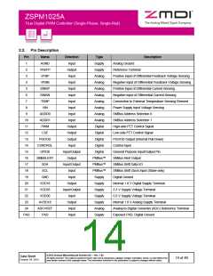
2.2. Pin Description
Pin
1
Name
AGND
VREFP
VFBP
Direction
Input
Type
Supply
Supply
Analog
Analog
Analog
Analog
Analog
Analog
Analog
Analog
Digital
Description
Analog Ground
2
Output
Input
Reference Terminal
3
Positive Input of Differential Feedback Voltage Sensing
Negative Input of Differential Feedback Voltage Sensing
Positive Input of Differential Current Sensing
Negative Input of Differential Current Sensing
Connection to External Temperature Sensing Element
Power Supply Input Voltage Sensing
SMBus Address Selection 0
4
VFBN
Input
5
ISNSP
ISNSN
TEMP
Input
6
Input
7
Input
8
VIN
Input
9
ADDR0
ADDR1
PWM
Input
10
11
12
13
14
15
16
17
18
19
20
21
22
23
24
PAD
Input
SMBus Address Selection 1
Output
Output
Output
Input
High-side FET Control Signal
LSE
Digital
Low-side FET Control Signal
PGOOD
CONTROL
GPIO0
SMBALERT
SDA
Digital
PGOOD Output (Internal Pull-Down)
Control Input
Digital
Input/Output
Output
Input/Output
Input
Digital
General Purpose Input/Output Pin
SMBus Alert Output
PMBus™
PMBus™
PMBus™
Supply
Supply
Supply
Supply
Supply
Analog
Supply
SMBus Shift Data I/O
SCL
SMBus Shift Clock Input (Slave-only)
Digital Ground
GND
Input
VDD18
VDD33
VDD50
AVDD18
ADCVREF
PAD
Output
Input/Output
Input
Internal 1.8 V Digital Supply Terminal
3.3 V Supply Voltage Terminal
5.0 V Supply Voltage Terminal
Output
Input
Internal 1.8 V Analog Supply Terminal
Analog-to-Digital Converter (ADC) Reference Terminal
Exposed PAD, Digital Ground
Input
© 2013 Zentrum Mikroelektronik Dresden AG — Rev. 1.00
All rights reserved. The material contained herein may not be reproduced, adapted, merged, translated, stored, or used without the
prior written consent of the copyright owner. The information furnished in this publication is subject to changes without notice.
Data Sheet
October 24, 2013
14 of 46

 ETC [ ETC ]