ZSPM1025A
True Digital PWM Controller (Single-Phase, Single-Rail)
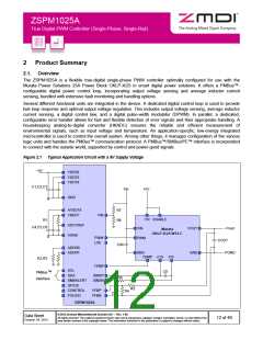
3
Functional Description
3.1. Power Supply Circuitry, Reference Decoupling, and Grounding
The ZSPM1025A incorporates several internal power regulators in order to derive all required supply and bias
voltages from a single external supply voltage. This supply voltage can be either 5 V or 3.3 V depending on
whether the internal 3.3 V regulator should be used. If the internal 3.3 V regulator is not used, 3.3 V must be
supplied to the 3.3 and 5 V supply pins. Decoupling capacitors are required at the VDD33, VDD18, and AVDD18
pins (1.0 µF minimum; 4.7 µF recommended). If the 5.0 V supply voltage is used, i.e. the internal 3.3 V regulator
is used, a small load current can be drawn from the VDD33 pin. This can be used to supply pull-up resistors, for
example.
The reference voltages required for the analog-to-digital converters are generated within the ZSPM1025A.
External decoupling must be provided between the VREFP and ADCVREF pins. Therefore, a 4.7 µF capacitor is
required at the VREFP pin and a 100 nF capacitor is required at the ADCVREF pin. The two pins should be
connected with approximately 50 Ω resistance in order to provide sufficient decoupling between the pins.
Three different ground connections (the pad, AGND pin, and GND pin) are available on the outside of the pack-
age. These should be connected together to a single ground tie. A differentiation between analog and digital
ground is not required.
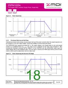
3.2. Reset/Start-up Behavior
The ZSPM1025A employs an internal power-on-reset (POR) circuit to ensure proper start up and shut down with
a changing supply voltage. Once the supply voltage increases above the POR threshold voltage, the ZSPM1025A
begins the internal start-up process. Upon its completion, the device is ready for operation.
3.3. Digital Power Control
3.3.1.
Overview
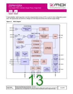
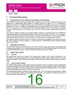
The digital power control loop consists of the integral parts required for the control functionality of the
ZSPM1025A. A high-speed analog front-end is used to digitize the output voltage. A digital control core uses the
acquired information to provide duty-cycle information to the PWM, which controls the drive signals to the power
stage.
3.3.2.
Output Voltage Feedback
The voltage feedback signal is sampled with a high-speed analog front-end. The feedback voltage is differentially
measured and subtracted from the voltage reference provided by a reference digital-to-analog converter (DAC)
using an error amplifier. A flash ADC is then used to convert the voltage into its digital equivalent. This is followed
by internal digital filtering to improve the system’s noise rejection.
An external feedback divider is required for output voltages above 1.20V. The reference DAC generates a voltage
up to 1.44 V. Keeping the voltage on the feedback pin (VFBP) below 1.20 V guarantees sufficient head room for
the output voltage compensation loop.
© 2013 Zentrum Mikroelektronik Dresden AG — Rev. 1.00
All rights reserved. The material contained herein may not be reproduced, adapted, merged, translated, stored, or used without the
prior written consent of the copyright owner. The information furnished in this publication is subject to changes without notice.
Data Sheet
October 24, 2013
16 of 46

 ETC [ ETC ]