TLV9001, TLV9002, TLV9004
www.ti.com
SBOS833A –OCTOBER 2017–REVISED DECEMBER 2017
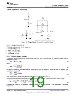
Typical Application (continued)
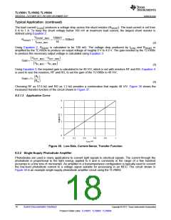
+3.3V
R1
11.5 kΩ
CF
10 pF
VREF
R2
357 Ω
RF
309 kΩ
+3.3V
œ
TLV9002
VOUT
+
VREF
CPD
47 pF
IIN
0-10 µA
RL
10 kꢀ
Copyright © 2017, Texas Instruments Incorporated
Figure 39. Single-Supply Photodiode Amplifier Circuit
8.2.2.1 Design Requirements
The design requirements for this design are:
•
•
•
•
Supply Voltage: 3.3 V
Input: 0 µA to 10 µA
Output: 0.1 V to 3.2 V
Bandwidth: 50 kHz
8.2.2.2 Detailed Design Procedure
The transfer function between the output voltage, VOUT, the input current, IIN, and the reference voltage, VREF, is
defined in Equation 5.
VOUT = IIN ìRF + VREF
(5)
Where
≈
∆
«
’
÷
R1 ìR2
R1 + R2 ◊
VREF = V ì
+
(6)
Set VREF to 100mV to meet the minimum output voltage level by setting R1 and R2 to meet the required ratio
calculated in Equation 7.
VREF
0.1 V
3.3 V
=
= 0.0303
V+
(7)
The closest resistor ratio to meet this ratio sets R1 to 11.5 kΩ and R2 to 357 Ω.
The required feedback resistance can be calculated based on the input current and desired output voltage.
VOUT - VREF
3.2 V - 0.1 V
10 mA
kV
A
RF =
=
= 310
ö 309 kW
I
IN
(8)
Calculate the value for the feedback capacitor based RF and the desired –3-dB bandwidth, f-3dB using
Equation 9.
Copyright © 2017, Texas Instruments Incorporated
Submit Documentation Feedback
19
Product Folder Links: TLV9001 TLV9002 TLV9004

 ETC [ ETC ]