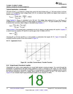
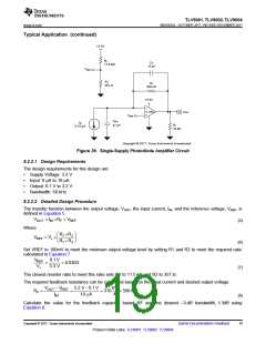
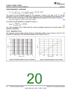
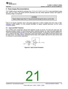
TLV9001, TLV9002, TLV9004
SBOS833A –OCTOBER 2017–REVISED DECEMBER 2017
www.ti.com
10 Layout
10.1 Layout Guidelines
For best operational performance of the device, use good printed circuit board (PCB) layout practices, including:
•
Noise can propagate into analog circuitry through the power pins of the circuit as a whole and of op amp
itself. Bypass capacitors are used to reduce the coupled noise by providing low-impedance power
sources local to the analog circuitry.
–
Connect low-ESR, 0.1-µF ceramic bypass capacitors between each supply pin and ground, placed as
close to the device as possible. A single bypass capacitor from V+ to ground is applicable for single-
supply applications.
•
•
Separate grounding for analog and digital portions of circuitry is one of the simplest and most-effective
methods of noise suppression. One or more layers on multilayer PCBs are usually devoted to ground
planes. A ground plane helps distribute heat and reduces electromagnetic interference (EMI) noise
pickup. Ensure to physically separate digital and analog grounds, paying attention to the flow of the
ground current. For more detailed information, see Circuit Board Layout Techniques.
In order to reduce parasitic coupling, run the input traces as far away from the supply or output traces as
possible. If these traces cannot be kept separate, crossing the sensitive trace perpendicular is much
better as opposed to in parallel with the noisy trace.
•
•
•
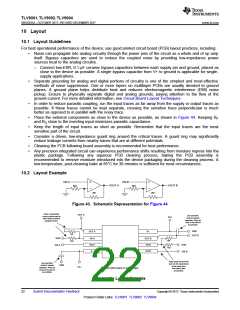
Place the external components as close to the device as possible, as shown in Figure 44. Keeping RF
and RG close to the inverting input minimizes parasitic capacitance.
Keep the length of input traces as short as possible. Remember that the input traces are the most
sensitive part of the circuit.
Consider a driven, low-impedance guard ring around the critical traces. A guard ring may significantly
reduce leakage currents from nearby traces that are at different potentials.
•
•
Cleaning the PCB following board assembly is recommended for best performance.
Any precision integrated circuit can experience performance shifts resulting from moisture ingress into the
plastic package. Following any aqueous PCB cleaning process, baking the PCB assembly is
recommended to remove moisture introduced into the device packaging during the cleaning process. A
low-temperature, post-cleaning bake at 85°C for 30 minutes is sufficient for most circumstances.
10.2 Layout Example
VIN A
VIN B
+
+
VOUT A
VOUT B
RG
RG
RF
RF
Figure 43. Schematic Representation for Figure 44
Place components
close to device and to
each other to reduce
parasitic errors.
OUT A
Use low-ESR,
ceramic bypass
capacitor. Place as
close to the device
as possible.
VS+
GND
OUT A
V+
RF
OUT B
GND
-IN A
+IN A
Vœ
OUT B
-IN B
RF
RG
GND
VIN B
VIN A
RG
+IN B
Keep input traces short
and run the input traces
as far away from
the supply lines
Use low-ESR,
GND
ceramic bypass
capacitor. Place as
close to the device
as possible.
VSœ
Ground (GND) plane on another layer
as possible.
Figure 44. Layout Example
22
Submit Documentation Feedback
Copyright © 2017, Texas Instruments Incorporated
Product Folder Links: TLV9001 TLV9002 TLV9004

 ETC [ ETC ]