TLV9001, TLV9002, TLV9004
SBOS833A –OCTOBER 2017–REVISED DECEMBER 2017
www.ti.com
7.3 Feature Description
7.3.1 Operating Voltage
The TLV900x series of op amps are ensured for operation from 1.8 V to 5.5 V. In addition, many specifications
apply from –40°C to +125°C. Parameters that vary significantly with operating voltages or temperature are
illustrated in the section.
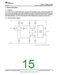
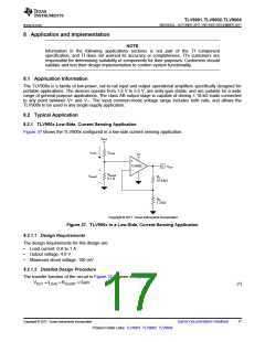
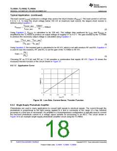
7.3.2 Rail-to-Rail Input
The input common-mode voltage range of the TLV900x family extends 100 mV beyond the supply rails for the
full supply voltage range of 1.8 V to 5.5 V. This performance is achieved with a complementary input stage: an
N-channel input differential pair in parallel with a P-channel differential pair, as shown in the Functional Block
Diagram. The N-channel pair is active for input voltages close to the positive rail, typically (V+) – 1.4 V to 100 mV
above the positive supply, whereas the P-channel pair is active for inputs from 100 mV below the negative
supply to approximately (V+) – 1.4 V. There is a small transition region, typically (V+) – 1.2 V to (V+) – 1 V, in
which both pairs are on. This 100-mV transition region can vary up to 100 mV with process variation. Thus, the
transition region (with both stages on) can range from (V+) – 1.4 V to (V+) – 1.2 V on the low end, and up to
(V+) – 1 V to (V+) – 0.8 V on the high end. Within this transition region, PSRR, CMRR, offset voltage, offset drift,
and THD can degrade compared to device operation outside this region.
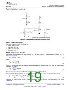
7.3.3 Rail-to-Rail Output
Designed as a low-power, low-voltage operational amplifier, the TLV900x series delivers a robust output drive
capability. A class AB output stage with common-source transistors achieves full rail-to-rail output swing
capability. For resistive loads of 10 kΩ, the output swings to within 20 mV of either supply rail, regardless of the
applied power-supply voltage. Different load conditions change the ability of the amplifier to swing close to the
rails.
7.3.4 Overload Recovery
Overload recovery is defined as the time required for the operational amplifier output to recover from a saturated
state to a linear state. The output devices of the operational amplifier enter a saturation region when the output
voltage exceeds the rated operating voltage, because of the high input voltage or the high gain. After the device
enters the saturation region, the charge carriers in the output devices require time to return to the linear state.
After the charge carriers return to the linear state, the device begins to slew at the specified slew rate. Therefore,
the propagation delay (in case of an overload condition) is the sum of the overload recovery time and the slew
time. The overload recovery time for the TLV900x series is approximately 850 ns.
7.4 Device Functional Modes
The TLV900x family has a single functional mode. The devices are powered on as long as the power-supply
voltage is between 1.8 V (±0.9 V) and 5.5 V (±2.75 V).
16
Submit Documentation Feedback
Copyright © 2017, Texas Instruments Incorporated
Product Folder Links: TLV9001 TLV9002 TLV9004

 ETC [ ETC ]