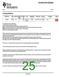
TLV9001, TLV9002, TLV9004
www.ti.com
SBOS833A –OCTOBER 2017–REVISED DECEMBER 2017
9 Power Supply Recommendations
The TLV900x series is specified for operation from 1.8 V to 5.5 V (±0.9 V to ±2.75 V); many specifications apply
from –40°C to +125°C. The section presents parameters that may exhibit significant variance with regard to
operating voltage or temperature.
CAUTION
Supply voltages larger than 6 V may permanently damage the device; see the table.
Place 0.1-µF bypass capacitors close to the power-supply pins to reduce coupling errors from noisy or high-
impedance power supplies. For more detailed information on bypass capacitor placement, see the Layout
Guidelines section.
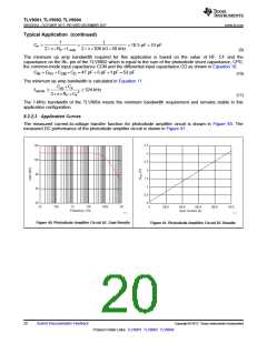
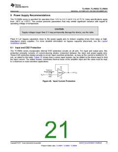
9.1 Input and ESD Protection
The TLV900x series incorporates internal ESD protection circuits on all pins. For input and output pins, this
protection primarily consists of current-steering diodes connected between the input and power-supply pins.
These ESD protection diodes provide in-circuit, input overdrive protection, as long as the current is limited to 10-
mA, as stated in the table. Figure 42 shows how a series input resistor can be added to the driven input to limit
the input current. The added resistor contributes thermal noise at the amplifier input and the value must be kept
to a minimum in noise-sensitive applications.
V+
IOVERLOAD
10-mA maximum
VOUT
Device
VIN
5 kW
Figure 42. Input Current Protection
Copyright © 2017, Texas Instruments Incorporated
Submit Documentation Feedback
21
Product Folder Links: TLV9001 TLV9002 TLV9004

 ETC [ ETC ]