BLF8G27LS-150(G)V
Power LDMOS transistor
5. Thermal characteristics
Table 5.
Thermal characteristics
Symbol Parameter
Conditions
Typ
Unit
Rth(j-c)
thermal resistance from junction to case Tcase = 80 C; PL = 45 W
0.30 K/W
6. Characteristics
Table 6.
DC characteristics
Tj = 25 C unless otherwise specified.
Symbol Parameter
V(BR)DSS drain-source breakdown voltage VGS = 0 V; ID = 2.16 mA
Conditions
Min Typ Max Unit
65
-
-
V
V
VGS(th)
IDSS
gate-source threshold voltage
drain leakage current
VDS = 10 V; ID = 216 mA
VGS = 0 V; VDS = 28 V
1.5 1.9 2.3
-
-
-
4.5 A
IDSX
drain cut-off current
VGS = VGS(th) + 3.75 V;
VDS = 10 V
40
-
A
IGSS
gfs
gate leakage current
VGS = 11 V; VDS = 0 V
VDS = 10 V; ID = 10.8 A
-
-
-
-
450 nA
forward transconductance
16
-
S
RDS(on)
drain-source on-state resistance VGS = VGS(th) + 3.75 V;
ID = 7.56 A
0.06 -
Table 7.
RF characteristics
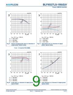
Test signal: 2-carrier W-CDMA, 3GPP test model; 64 DPCH; PAR = 8.4 dB at 0.01 % probability on
the CCDF, carrier spacing 5 MHz; f1 = 2602.5 MHz; f2 = 2607.5 MHz; f3 = 2692.5 MHz;
f4 = 2697.5 MHz; RF performance at VDS = 28 V; IDq = 1300 mA; Tcase = 25 C; unless otherwise
specified; in a class-AB production test circuit.
Symbol Parameter
Conditions
Min
16.8
-
Typ Max
18
10 7
30
30 26
Unit
dB
Gp
power gain
PL(AV) = 45 W
PL(AV) = 45 W
PL(AV) = 45 W
-
RLin
D
input return loss
drain efficiency
dB
26
-
-
%
ACPR5M adjacent channel power ratio (5 MHz) PL(AV) = 45 W
dBc
7. Test information
7.1 Ruggedness in class-AB operation
The BLF8G27LS-150V and BLF8G27LS-150GV are capable of withstanding a load
mismatch corresponding to VSWR = 10 : 1 through all phases under the following
conditions: VDS = 28 V; IDq = 1300 mA; PL = 150 W (CW); f = 2600 MHz.
BLF8G27LS-150V_8G27LS-150GV#4
All information provided in this document is subject to legal disclaimers.
© Ampleon The Netherlands B.V. 2015. All rights reserved.
Product data sheet
Rev. 4 — 1 September 2015
3 of 17

 ETC [ ETC ]