BLF8G27LS-150(G)V
Power LDMOS transistor
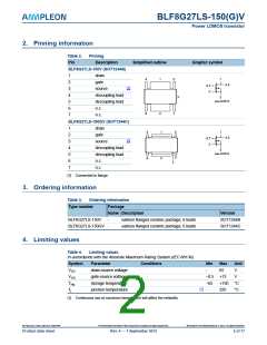
2. Pinning information
Table 2.
Pin
Pinning
Description
Simplified outline
Graphic symbol
BLF8G27LS-150V (SOT1244B)
1
2
3
4
5
6
7
drain
4
1
5
1
gate
4,5
6,7
2
[1]
source
decoupling lead
decoupling lead
n.c.
3
3
aaa-003619
6
2
7
n.c.
BLF8G27LS-150GV (SOT1244C)
1
2
3
4
5
6
7
drain
4
1
5
1
gate
4,5
6,7
2
[1]
source
decoupling lead
decoupling lead
n.c.
3
aaa-003619
6
2
7
3
n.c.
[1] Connected to flange.
3. Ordering information
Table 3.
Ordering information
Type number
Package
Name Description
Version
BLF8G27LS-150V
-
earless flanged ceramic package; 6 leads
earless flanged ceramic package; 6 leads
SOT1244B
SOT1244C
BLF8G27LS-150GV -
4. Limiting values
Table 4.
Limiting values
In accordance with the Absolute Maximum Rating System (IEC 60134).
Symbol
VDS
Parameter
Conditions
Min
Max
Unit
V
drain-source voltage
gate-source voltage
storage temperature
junction temperature
-
65
VGS
Tstg
0.5 +13
V
65
+150 C
[1]
Tj
-
225
C
[1] Continuous use at maximum temperature will affect the reliability.
BLF8G27LS-150V_8G27LS-150GV#4
All information provided in this document is subject to legal disclaimers.
© Ampleon The Netherlands B.V. 2015. All rights reserved.
Product data sheet
Rev. 4 — 1 September 2015
2 of 17

 ETC [ ETC ]