Epson Research and Development
Page 59
Vancouver Design Center
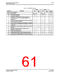
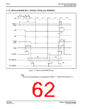
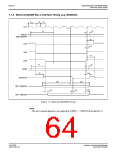
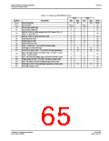
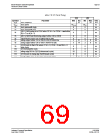
Table 7-6: Motorola MC68030 Timing
3.0V
5.0V
Symbol
Parameter
Min
Max
Min
Max
Units
MHz
ns
fCLK
TCLK
t2
Clock frequency
50
50
Clock period
1/fCLK
1/fCLK
Clock pulse width high
Clock pulse width low
6
6
6
6
ns
t3
ns
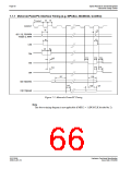
A[20:0], SIZ[1:0], M/R# setup to first CLK where CS# = 0,
AS# = 0, and DS# = 0
t4
5
3
ns
t5
t6
A[20:0], SIZ[1:0], M/R# hold from AS#
CS# hold from AS#
0
0
0
0
ns
ns
ns
ns
ns
ns
ns
t7
R/W# setup to DS#
10
0
10
0
t8
R/W# hold from AS#
t9
AS# = 0 and CS# = 0 to DSACK1# driven high
AS# high to DSACK1# high
1
1
t10
t11
4
18
15
3
12
14
First BCLK where AS# = 1 to DSACK1# high impedance
3
2
D[31:16] valid to third CLK where CS# = 0, AS# = 0, and
DS# = 0 (write cycle)
t12
0
0
ns
t13
t14
t15
t16
t17
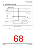
D[31:16] hold from falling edge of DSACK1# (write cycle)
Falling edge of DS# = 0 to D[31:16] driven (read cycle)
D[31:16] valid to DSACK1# falling edge (read cycle)
DS# high to D[31:16] invalid/high impedance (read cycle)
AS# high setup to CLK
0
3
0
6
4
0
3
0
4
3
ns
ns
ns
ns
ns
31
15
Hardware Functional Specification
Issue Date: 01/02/06
S1D13506
X25B-A-001-10

 EPSON [ EPSON COMPANY ]