Epson Research and Development
Page 13
Vancouver Design Center
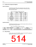
4.2 Non-PCI Host Interface Support
The S5U13506B00C is specifically designed to support a standard PCI bus environment
(using the PCI Bridge Adapter FPGA). However, the S5U13506B00C can directly support
many other Host Bus Interfaces. When the FPGA is disabled (using jumper JP9), headers
H1 and H2 provide the necessary IO pins to interface to the Host Bus Interfaces listed in
Table 4-4:, “CPU Interface Pin Mapping”. The S1D13506 power supply must be set to
3.3V or 5V (using jumper JP1) according to the host CPU signalling voltage.
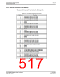
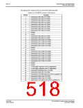
4.2.1 CPU Interface Pin Mapping
The functions of the S1D13506 host interface pins are mapped to each host bus interface
according to the following table.
Table 4-4: CPU Interface Pin Mapping
S1D1350
6
Pin
Names
Motorola Motorola
Philips
PR31500
/PR31700
Hitachi
SH-4/SH-3
Motorola
PowerPC
Toshiba
TX3912
Generic
MIPS/ISA MC68K
MC68K
Bus 2
PC Card
Bus 1
AB20
AB19
AB18
AB17
A20
A19
A18
A17
A20
A19
LatchA20
SA19
A20
A19
A18
A17
A20
A19
A11
A12
A13
A14
A20
A19
A18
A17
ALE
ALE
/CARDREG
CARDREG*
A18
SA18
A18
/CARDIORD CARDIORD*
/CARDIOWR CARDIOWR*
Connected to VDD
A17
SA17
A17
AB[16:13] A[16:13]
AB[12:1] A[12:1]
A[16:13]
A[12:1]
A01
SA[16:13] A[16:13]
A[16:13]
A[12:1]
A0
A[15:18] A[16:13]
SA[12:1]
SA0
A[12:1]
LDS#
A[19:30]
A31
A[12:1]
A01
A[12:1]
A0
A[12:1]
A0
AB0
DB[15:8] D[15:0]
A01
D[15:8]
D[7:0]
WE1#
SD[15:0]
SD[7:0]
SBHE#
D[15:8]
D[7:0]
UDS#
D[31:24]
D[23:16]
DS#
D[0:7]
D[8:15]
BI
D[15:0]
D[7:0]
-CE2
D[23:16]
D[31:24]
D[23:16]
D[31:24]
DB[7:0]
WE1#
M/R#
D[7:0]
WE1#
/CARDxCSH CARDxCSH*
Connected to VDD
External Decode
External Decode
CLK
CS#
Connected to VDD
BUSCLK
BCLK
CKIO
BS#
CLK
CLK
AS#
CLKOUT
TS
CLK
DCLKOUT
Connected to VDD
/CARDxCSL CARDxCSL*
DCLKOUT
Connected
to VDD
Connected to
VDD
Connected
to VDD
BS#
RD/WR#
RD#
AS#
Connected to
VDD
RD1#
RD0#
WE0#
RD/WR#
RD#
R/W#
R/W#
SIZ1
SIZ0
RD/WR
TSIZ0
TSIZ1
-CE1
-OE
Connected
to VDD
MEMR#
MEMW#
/RD
RD*
WE*
Connected
to VDD
WE0#
WE0#
-WE
/WE
RDY#
/WAIT#
WAIT#
WAIT#
IOCHRDY DTACK# DSACK1#
inverted
TA
-WAIT /CARDxWAIT CARDxWAIT*
inverted
RESET# RESET# RESET#
RESET# RESET# RESET#
RESET#
PON*
RESET
RESET
S5U13506B00C Evaluation Board User Manual
Issue Date: 01/02/06
S1D13506
X25B-G-004-06

 EPSON [ EPSON COMPANY ]