Page 12
Epson Research and Development
Vancouver Design Center
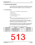
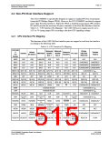
4.1.1 On-Board PCI Configuration Registers
Read-Only Registers
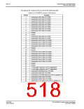
The PCI Bridge Adapter FPGA provides configuration registers which contain
identification information required by the PCI interface. The following values are
hard-wired into these registers.
Table 4-2: PCI Configuration Register Read Values
Name
Vendor ID
Address
0h
Register size
16 bits
16 bits
16 bits
8 bits
Value
10F4h
1300h
400h
1
Device ID
2h
Status
6h
Revision ID
Class Code
Subsystem Vendor ID
Subsystem ID
Header Type
n/a
8h
9h
24 bits
16 bits
16 bits
8 bits
FF 0000h
10F4h
8000h
0
2Ch
2Dh
Eh
Fh-FFh
32 bits
0
Read/Write Registers
The PCI Bridge Adapter FPGA provides two read/write registers which are used for access
enabling and memory mapping as follows.
Table 4-3: PCI Configuration Register Write Values
Name
Address Register size
Valid bits
Meaning
Command
4h
16 bits
32 bits
Bit 1 only; other bits are zero.
Bits 31 to 22; other bits are zero.
Access enabled if high
Base Address
10h
Position of 4M byte reserved window
4.1.2 Utility Software
All utility software for the S5U13506B00C evaluation board is fully PCI compliant and
handles the PCI configuration registers automatically.
S1D13506
X25B-G-004-06
S5U13506B00C Evaluation Board User Manual
Issue Date: 01/02/06

 EPSON [ EPSON COMPANY ]