Epson Research and Development
Page 11
Vancouver Design Center
4 Technical Description
The S5U13506B00C operates with both PCI and non-PCI evaluation platforms. It supports
display types such as, passive LCD panels (4/8/16-bit), TFT/D-TFD panels (9/12/18-bit),
CRT and TV (NTSC and PAL). Additionally, it supports a variety of clock options.
4.1 PCI Bus Support
As a PCI device, the S5U13506B00C has the following characteristics.
• 33MHz bus clock.
• Target with no interrupts.
• Non-cacheable memory read and write.
• 3.3V or 5V PCI signalling.
Note
In a 3.3V PCI system, the S1D13506 must be powered at 3.3V by setting jumper JP1. In
a 5V PCI system, the S1D13506 may be powered at either 3.3V or 5V.
Although the S1D13506 does not support the PCI bus directly, the S5U13506B00C
supports the PCI bus using a PCI Bridge Adapter FPGA. The FPGA translates PCI accesses
into PC Card accesses which are then decoded by the S1D13506.
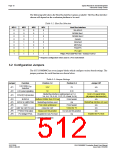
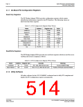
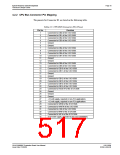
A 4M byte PCI address range is allocated to the S5U13506B00C by the system BIOS. The
S1D13506 uses this address range to map the internal registers and the 2M byte display
buffer. The following table shows the memory mapping of the PCI address block.
Table 4-1: S1D13506 Memory Mapping onto 4M byte PCI Address Block
PCI Memory Offset
00 0000h to 00 01FFh
00 1000h to 00 1FFFh
10 0000h to 1F FFFFh
20 0000h to 3F FFFFh
Description
S1D13506 M/R#
S1D13506 AB[20:0]
00 0000h to 00 01FFh
00 1000h to 00 1FFFh
10 0000h to 1F FFFFh
00 0000h to 1F FFFFh
General registers (512 byte)
MediaPlug registers (4K byte)
BitBlt data registers (1M byte)
Display Buffer (2M byte)
0
0
0
1
S5U13506B00C Evaluation Board User Manual
Issue Date: 01/02/06
S1D13506
X25B-G-004-06

 EPSON [ EPSON COMPANY ]