Page 16
Epson Research and Development
Vancouver Design Center
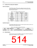
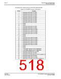
The pinouts for Connector H2 are listed in the following table.
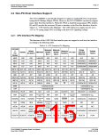
Table 4-6: CPU/BUS Connector (H2) Pinout
Pin No.
1
Function
Connected to AB0 of the S1D13506
Connected to AB1 of the S1D13506
Connected to AB2 of the S1D13506
Connected to AB3 of the S1D13506
Connected to AB4 of the S1D13506
Connected to AB5 of the S1D13506
Connected to AB6 of the S1D13506
Connected to AB7 of the S1D13506
Ground
2
3
4
5
6
7
8
9
10
11
12
13
14
15
16
17
18
19
20
21
22
23
24
25
26
27
28
29
30
31
32
33
34
Ground
Connected to AB8 of the S1D13506
Connected to AB9 of the S1D13506
Connected to AB10 of the S1D13506
Connected to AB11 of the S1D13506
Connected to AB12 of the S1D13506
Connected to AB13 of the S1D13506
Ground
Ground
Connected to AB14 of the S1D13506
Connected to AB15 of the S1D13506
Connected to AB16 of the S1D13506
Connected to AB17 of the S1D13506
Connected to AB18 of the S1D13506
Connected to AB19 of the S1D13506
Ground
Ground
+5 volt supply, required in non-PCI applications
+5 volt supply, required in non-PCI applications
Connected to RD/WR# of the S1D13506
Connected to BS# of the S1D13506
Connected to S1D13506 BUSCLK if JP4 is in position 2-3
Connected to RD# of the S1D13506
Connected to AB20 of the S1D13506
Connected to S1D13506 CLKI if JP6 is in position 2-3
S1D13506
X25B-G-004-06
S5U13506B00C Evaluation Board User Manual
Issue Date: 01/02/06

 EPSON [ EPSON COMPANY ]