Epson Research and Development
Page 21
Vancouver Design Center
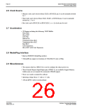
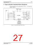
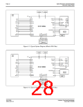
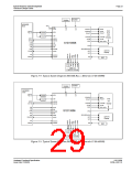
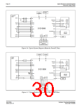
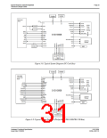
3 Typical System Implementation Diagrams
For the pin mapping of each system implementation, see Table 5-7:, “CPU Interface Pin
Mapping,” on pag e40.
.
Oscillator
Oscillator
Generic
BUS
VDD
BS#
A0
FPDAT[7:4]
FPSHIFT
L[3:0]
4-bit
Single
FPSHIFT
M/R#
CS#
A[27:21]
CSn#
Decoder
LCD
FPFRAME
FPLINE
DRDY
FPFRAME
FPLINE
Display
A[20:1]
D[15:0]
AB[20:1]
DB[15:0]
DRDY (MOD)
S1D13506
WE0#
WE1#
WE0#
WE1#
GPIOx
RD0#
RD1#
RD#
RED,GREEN,BLUE
HRTC
RD/WR#
WAIT#
CRT/TV
Display
WAIT#
VRTC
BCLK
BUSCLK
RESET#
IREF
RESET#
IREF
1Mx16
FPM/EDO-DRAM
Figure 3-1: Typical System Diagram (Generic Bus)
Hardware Functional Specification
Issue Date: 01/02/06
S1D13506
X25B-A-001-10

 EPSON [ EPSON COMPANY ]