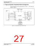
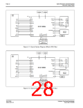
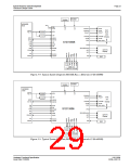
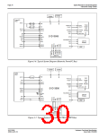
Page 20
Epson Research and Development
Vancouver Design Center
2.6 Clock Source
• Memory clock can be derived from CLKI or BUSCLK pin. It can be internally divided
by 2.
• Pixel clock can be derived from CLKI, CLKI2, or BUSCLK pin. It can be internally
divided by 2, 3 or 4.
• Bus clock can be BUSCLK or (BUSCLK)/2, i.e. a 2x clock may be used.
2.7 Acceleration
• 2D Engine including the following 2 ROP BitBlts:
Write BLT.
Move BLT.
Solid Fill.
Pattern Fill.
Transparent Write BLT.
Transparent Move BLT.
Read BLT.
Color Expansion.
Move BLT with Color Expansion.
2.8 MediaPlug Interface
• Built-in WINNOV MediaPlug interface.
• Videum®Cam support at resolution of 320x240x256 color at 30fps.
2.9 Miscellaneous
• The memory data bus, MD[15:0], is used to configure the chip at power-on.
• Three General Purpose Input/Output pins, GPIO[3:1], are available if upper Memory
Address pins are not required for asymmetric DRAM support.
• Power save mode is initiated by software.
• Operating voltage from 2.7 volts to 5.5 volts.
• 128-pin QFP15 surface mount package.
S1D13506
X25B-A-001-10
Hardware Functional Specification
Issue Date: 01/02/06

 EPSON [ EPSON COMPANY ]