Epson Research and Development
Page 139
Vancouver Design Center
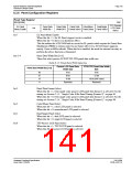
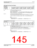
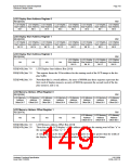
LCD Vertical Non-Display Period Register
REG[03Ah]
RW
LCD Vertical
LCD Vertical LCD Vertical LCD Vertical LCD Vertical LCD Vertical LCD Vertical
Non-Display
Period Status
(RO)
n/a
Non-Display
Period Bit 5
Non-Display
Period Bit 4
Non-Display
Period Bit 3
Non-Display
Period Bit 2
Non-Display
Period Bit 1
Non-Display
Period Bit 0
bit 7
LCD Vertical Non-Display Period Status
This is a read-only status bit.
When a read from this bit = 1, a LCD panel vertical non-display period is occurring.
When a read from this bit = 0, the LCD panel output is in a vertical display period.
bits 5-0
LCD Vertical Non-Display Period Bits [5:0]
These bits specify the LCD panel vertical non-display period height in 1 line resolution.
Vertical non-display period height in number of lines = (ContentsOfThisRegister) + 1
Note
For TFT/D-TFD only:
(REG[03Ah] bits 5-0 + 1) ≥ (REG[03Bh] + 1) + (REG[03Ch] bits 2-0 + 1)
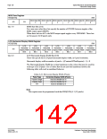
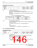
TFT FPFRAME Start Position Register
REG[03Bh]
RW
TFT
FPFRAME
TFT
FPFRAME
TFT
FPFRAME
TFT
FPFRAME
TFT
FPFRAME
TFT
FPFRAME
n/a
n/a
Start Position Start Position Start Position Start Position Start Position Start Position
Bit 5 Bit 4 Bit 3 Bit 2 Bit 1 Bit 0
bits 5-0
TFT FPFRAME Start Position Bits [5:0]
For TFT/D-TFD panel only, these bits specify the delay in lines from the start of the ver-
tical non-display period to the leading edge of the FPFRAME pulse.
FPFRAME start position in number of lines = (ContentsOfThisRegister) + 1
Note
For TFT/D-TFD only:
(REG[03Ah] bits 5-0 + 1) ≥ (REG[03Bh] + 1) + (REG[03Ch] bits 2-0 + 1)
Hardware Functional Specification
Issue Date: 01/02/06
S1D13506
X25B-A-001-10

 EPSON [ EPSON COMPANY ]