Page 118
Epson Research and Development
Vancouver Design Center
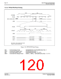
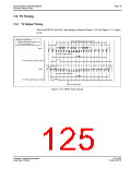
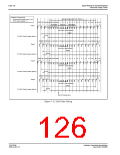
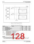
t1
t2
VRTC
t3
HRTC
Figure 7-49: CRT A.C. Timing
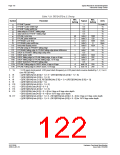
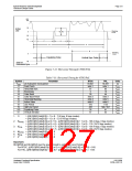
Table 7-34: CRT A.C. Timing
Min.
Setting
Max.
Symbol
Parameter
Typical
Units
Setting
1152
8
t1
t2
t3
VRTC cycle time
2
1
8
note 1
note 2
note 3
lines
lines
Ts
VRTC pulse width low
VRTC falling edge to FPLINE falling edge phase difference
512
1. t1
2. t2
3. t3
= [((REG[057h] bits 1:0, REG[056h] bits 7:0) + 1) + ((REG[058h] bits 6:0) + 1)] lines
= [((REG[05Ah] bits 2:0) + 1)] lines
= [((REG[053h] bits 5:0) + 1) × 8] Ts
S1D13506
X25B-A-001-10
Hardware Functional Specification
Issue Date: 01/02/06

 EPSON [ EPSON COMPANY ]