Page 116
Epson Research and Development
Vancouver Design Center
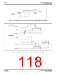
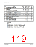
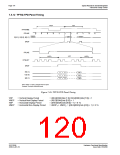
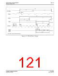
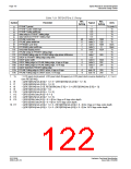
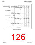
Table 7-33: TFT/D-TFD A.C. Timing
Min.
Setting
Max.
Setting
Symbol
Parameter
Typical
Units
FPSHIFT period
FPSHIFT pulse width high
FPSHIFT pulse width low
data setup to FPSHIFT falling edge
data hold from FPSHIFT falling edge
FPLINE cycle time
FPLINE pulse width low
FPFRAME cycle time
FPFRAME pulse width low
horizontal display period
FPLINE setup to FPSHIFT falling edge
FPFRAME falling edge to FPLINE falling edge phase difference
DRDY to FPSHIFT falling edge setup time
DRDY pulse width
DRDY falling edge to FPLINE falling edge, 4 bpp or 8 bpp
DRDY falling edge to FPLINE falling edge, 15/16 bpp
DRDY hold from FPSHIFT falling edge
FPLINE Falling edge to DRDY active, 4 bpp or 8 bpp
FPLINE Falling edge to DRDY active, 15/16 bpp
1
0.5
0.5
0.5
Ts (note 1)
Ts
t1
t2
t3
t4
t5
t6
t7
t8
t9
t10
t11
t12
t13
Ts
Ts
Ts
Ts
0.5
40
8
2
1
8
note 2
note 3
note 4
note 5
note 6
0.5
note 7
0.5
note 8
note 9
note 9
0.5
1280
128
1088
8
Ts
lines
lines
Ts
Ts
Ts
Ts
Ts
Ts
Ts
1024
1
249
t14
8
4
6
1024
252
254
t15a
t15b
t16
t17a
t17b
Ts
Ts
Ts
-6
-8
note 10
note 10
250
248
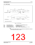
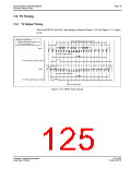
1. Ts
= LCD pixel clock period. LCD pixel clock frequency is LCD pixel clock source divided by 1, 2, 3 or 4
(see REG[014h]).
2. t6
3. t7
= [((REG[032h] bits [6:0]) + 1) × 8 + ((REG[034h] bits [4:0]) + 1) × 8]
= [((REG[036h] bits [3:0]) + 1) × 8]
4. t8
5. t9
= [((REG[039h] bits [1:0], REG[038h] bits [7:0]) + 1) + ((REG[03Ah] bits [5:0]) + 1)]
= [((REG[03Ch] bits [2:0]) + 1)]
6. t10
7. t12
8. t14
9. t15
= [((REG[032h] bits [6:0]) + 1) × 8]
= [(REG[035h] bits [4:0]) × 8 + 1]
= [((REG[032h] bits [6:0]) + 1) × 8]
= [(REG[035h] bits [4:0]) × 8 + 4] for 4 bpp or 8 bpp color depth
= [(REG[035h] bits [4:0]) × 8 + 6] for 15/16 bpp color depth
= [((REG[034h] bits [4:0]) + 1) × 8 - (REG[035h] bits [4:0]) × 8 - 4] for 4 bpp or 8 bpp color depth
= [((REG[034h] bits [4:0]) + 1) × 8 - (REG[035h] bits [4:0]) × 8 - 6] for 15/16 bpp color depth
10. t17
S1D13506
X25B-A-001-10
Hardware Functional Specification
Issue Date: 01/02/06

 EPSON [ EPSON COMPANY ]