DA14580
FINAL
Bluetooth Low Energy 4.2 SoC
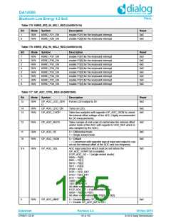
Table 177: GP_ADC_CTRL_REG (0x50001500)
Bit
Mode Symbol
Description
Reset
4
R
GP_ADC_INT
1 = AD conversion ready and has generated an interrupt.
Must be cleared by writing any value to
GP_ADC_CLEAR_INT_REG.
0x0
3
R/W
GP_ADC_CLK_SEL
0 = Internal high-speed ADC clock used.
1 = Digital clock used.
0x0
2
1
-
GP_ADC_TEST
GP_ADC_START
Reserved, keep 0.
0x0
0x0
R/W
0 = ADC conversion ready.
1 = If a 1 is written, the ADC starts a conversion. After the
conversion this bit will be set to 0 and the GP_ADC_INT bit
will be set.
0
R/W
GP_ADC_EN
0 = ADC is disabled and in reset.
0x0
1 = ADC is enabled and sampling of input is started.
Table 178: GP_ADC_CTRL2_REG (0x50001502)
Bit
15:4
3
Mode Symbol
Description
Reset
0x0
-
-
Reserved
R/W
GP_ADC_I20U
Adds 20uA constant load current at the ADC LDO to mini-
mize ripple on the reference voltage of the ADC.
0x0
2
1
R/W
R/W
GP_ADC_IDYN
Enables dynamic load current at the ADC LDO to minimize
ripple on the reference voltage of the ADC.
0x0
0x0
GP_ADC_ATTN3X
0 = Input voltages up to 1.2V allowed.
1 = Input voltages up to 3.6V allowed by enabling 3x attenu-
ator.
0
R/W
GP_ADC_DELAY_E
N
Enables delay function for several signals. This is not auto-
cleared. Toggle this bit before every sampling to enable suc-
cesive conversions.
0x0
Table 179: GP_ADC_OFFP_REG (0x50001504)
Bit
Mode Symbol
Description
Reset
0x0
15:10
9:0
-
-
Reserved
R/W
GP_ADC_OFFP
Offset adjust of 'positive' array of ADC-network (effective if
"GP_ADC_SE=0", or "GP_ADC_SE=1 AND
GP_ADC_SIGN=0")
0x200
Table 180: GP_ADC_OFFN_REG (0x50001506)
Bit
Mode Symbol
Description
Reset
0x0
15:10
9:0
-
-
Reserved
R/W
GP_ADC_OFFN
Offset adjust of 'negative' array of ADC-network (effective if
"GP_ADC_SE=0", or "GP_ADC_SE=1 AND
GP_ADC_SIGN=1")
0x200
Table 181: GP_ADC_CLEAR_INT_REG (0x50001508)
Bit
Mode Symbol
R0/W GP_ADC_CLR_INT
Description
Reset
15:0
Writing any value to this register will clear the ADC_INT
interrupt. Reading returns 0.
0x0
Datasheet
Revision 3.4
09-Nov-2016
CFR0011-120-01
116 of 155
© 2014 Dialog Semiconductor

 DIALOG [ Dialog Semiconductor ]