DA14580
FINAL
Bluetooth Low Energy 4.2 SoC
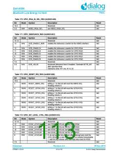
Table 182: GP_ADC_RESULT_REG (0x5000150A)
Bit
Mode Symbol
Description
Reset
15:10
9:0
-
-
Reserved
0x0
0x0
R
GP_ADC_VAL
Returns the 10 bits linear value of the last AD conversion.
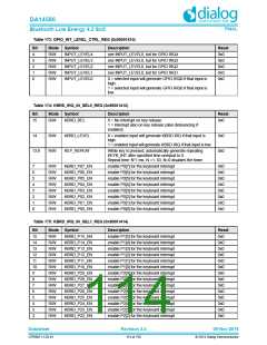
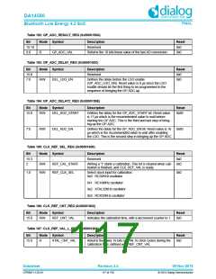
Table 183: GP_ADC_DELAY_REG (0x5000150C)
Bit
Mode Symbol
Description
Reset
0x0
15:8
7:0
-
-
Reserved
R/W
DEL_LDO_EN
Defines the delay before the LDO enable
0x0
(GP_ADC_LDO_EN). Reset value is 0 µs since the LDO
enable should be the first thing to be programmed in the
sequence of bringing the GP ADC up.
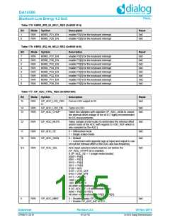
Table 184: GP_ADC_DELAY2_REG (0x5000150E)
Bit
Mode Symbol
Description
Reset
15:8
R/W
DEL_ADC_START
Defines the delay for the GP_ADC_START bit. Reset value
is 17 µs which is the recommended value to wait before
starting the GP ADC. This is the third and last step of bring-
ing up the GP ADC
0x88
7:0
R/W
DEL_ADC_EN
Defines the delay for the GP_ADC_EN bit. Reset value is 16
µs which is the recommended value to wait after enabling
the LDO. This is the second step in bringing up the GP ADC.
0x80
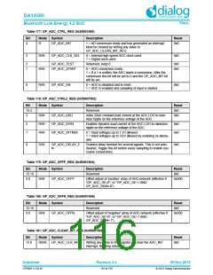
Table 185: CLK_REF_SEL_REG (0x50001600)
Bit
15:3
2
Mode Symbol
Description
Reset
-
-
Reserved
0x0
R/W
REF_CAL_START
Writing a '1' starts a calibration. This bit is cleared when cali- 0x0
bration is finished, and CLK_REF_VAL is ready.
1:0
R/W
REF_CLK_SEL
Select clock input for calibration:
0x0 : RC32KHz oscillator
0x0
0x1 : RC16MHz oscillator
0x2 : XTAL32KHz oscillator
0x3 : RCX32KHz oscillator
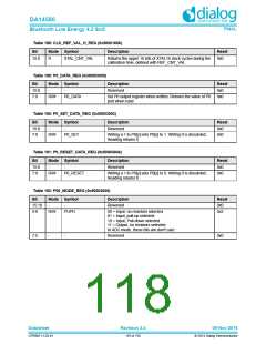
Table 186: CLK_REF_CNT_REG (0x50001602)
Bit
Mode Symbol
R/W REF_CNT_VAL
Description
Reset
15:0
Indicates the calibration time, with a decrement counter to 1.
0x0
Table 187: CLK_REF_VAL_L_REG (0x50001604)
Bit
Mode Symbol
XTAL_CNT_VAL
Description
Reset
15:0
R
Returns the lower 16 bits of XTAL16 clock cycles during the
calibration time, defined with REF_CNT_VAL
0x0
Datasheet
Revision 3.4
09-Nov-2016
CFR0011-120-01
117 of 155
© 2014 Dialog Semiconductor

 DIALOG [ Dialog Semiconductor ]