DA14580
FINAL
Bluetooth Low Energy 4.2 SoC
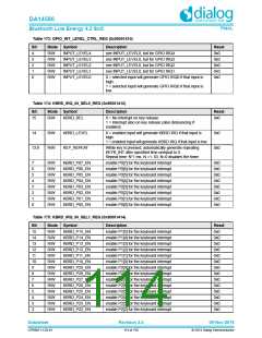
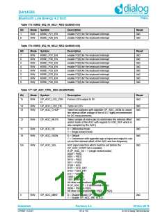
Table 175: KBRD_IRQ_IN_SEL1_REG (0x50001414)
Bit
1
Mode Symbol
Description
Reset
R/W
R/W
KBRD_P21_EN
KBRD_P20_EN
enable P2[1] for the keyboard interrupt
enable P2[0] for the keyboard interrupt
0x0
0x0
0
Table 176: KBRD_IRQ_IN_SEL2_REG (0x50001416)
Bit
7
Mode Symbol
Description
Reset
0x0
0x0
0x0
0x0
0x0
0x0
0x0
0x0
R/W
R/W
R/W
R/W
R/W
R/W
R/W
R/W
KBRD_P37_EN
enable P3[7] for the keyboard interrupt
enable P3[6] for the keyboard interrupt
enable P3[5] for the keyboard interrupt
enable P3[4] for the keyboard interrupt
enable P3[3] for the keyboard interrupt
enable P3[2] for the keyboard interrupt
enable P3[1] for the keyboard interrupt
enable P3[0] for the keyboard interrupt
6
KBRD_P36_EN
KBRD_P35_EN
KBRD_P34_EN
KBRD_P33_EN
KBRD_P32_EN
KBRD_P31_EN
KBRD_P30_EN
5
4
3
2
1
0
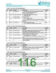
Table 177: GP_ADC_CTRL_REG (0x50001500)
Bit
Mode Symbol
Description
Reset
15
R/W
GP_ADC_LDO_ZER
Forces LDO-output to 0V.
0x0
O
14
13
R/W
R/W
GP_ADC_LDO_EN
GP_ADC_CHOP
Turns on LDO.
0x0
0x0
Takes two samples with opposite GP_ADC_SIGN to cancel
the internal offset voltage of the ADC; Highly recommended
for DC-measurements.
12
R/W
GP_ADC_MUTE
Takes sample at mid-scale (to dertermine the internal offset
and/or noise of the ADC with regards to VDD_REF which is
also sampled by the ADC).
0x0
11
10
R/W
R/W
GP_ADC_SE
0 = Differential mode
1 = Single ended mode
0x0
0x0
GP_ADC_SIGN
0 = Default
1 = Conversion with opposite sign at input and output to can-
cel out the internal offset of the ADC and low-frequency
9:6
R/W
GP_ADC_SEL
ADC input selection which must be set before the
GP_ADC_START bit is enabled.
If GP_ADC_SE = 1 (single ended mode):
0000 = P0[0]
0x0
0001 = P0[1]
0010 = P0[2]
0011 = P0[3]
0100 = AVS
0101 = VDD_REF
0110 = VDD_RTT
0111 = VBAT3V
1000 = VDCDC
1001 = VBAT1V
All other combinations are reserved.
If GP_ADC_SE = 0 (differential mode):
0000 = P0[0] vs P0[1]
All other combinations are P0[2] vs P0[3].
5
R/W
GP_ADC_MINT
0 = Disable (mask) GP_ADC_INT.
1 = Enable GP_ADC_INT to ICU.
0x0
Datasheet
Revision 3.4
09-Nov-2016
CFR0011-120-01
115 of 155
© 2014 Dialog Semiconductor

 DIALOG [ Dialog Semiconductor ]