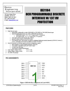
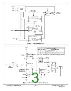
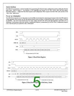
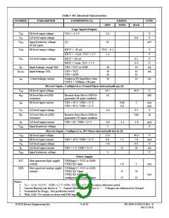
FUNCTIONAL DESCRIPTION
DEI1184 is an eight-channel discrete-to digital interface IC implemented in an HV DIMOS technology. It senses eight discrete
signals of the type commonly found in avionic systems and converts them to serial logic data. Each input can be individually
configured as either GND/OPEN or 28V/OPEN format input via a serial data input. The discrete data is read from the device via
an eight-bit serial shift register with 3-state output. This serial interface is compatible with the industry standard Serial Peripheral
Interface (SPI) bus.
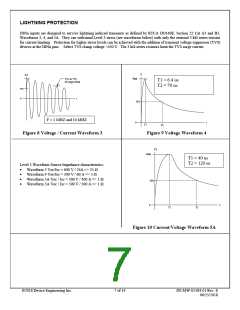
The discrete input circuits are designed to achieve a high level of lightning transient immunity. The application design provides
a series 3 kΩ resistor on each discrete input to achieve DO160E Level 3 and WF5A 500 V immunity. Higher immunity levels
can be achieved (i.e. Level 5) with the addition of a TVS between the resistor and the input pin.
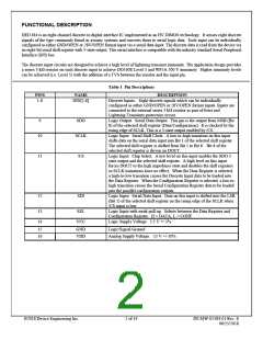
Table 1 Pin Descriptions
PINS
NAME
DESCRIPTION
1-8
DIN[1:8]
Discrete Inputs. Eight discrete signals which can be individually
configured as either GND/OPEN or 28V/OPEN format inputs. Inputs are
connected to the external series 3 kΩ resistor as part of front end
Lightning Transients protection circuit.
9
SDO
Logic Output. Serial Data Output. This pin is the output from MSB (Bit
8) of the selected shift register (Data/Configuration). It is clocked by the
rising edge of SCLK. This is a 3-state output enabled by /CS.
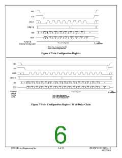
Logic Input. Serial Shift Clock. A low-to-high transition on this input
shifts data on the serial data input into Bit 1 of the selected shift register.
The selected shift register is shifted from Bit 1 to Bit 8. Bit 8 of the
selected shift register is driven on DOUT.
10
SCLK
11
12
/CS
SDI
Logic Input. Chip Select. A low level on this input enables the SDO 3-
state output and the selected shift register. A high level on this input
forces DOUT to the high impedance state and disables the shift registers
so SCLK transitions have no effect. When the Data Register is selected,
a high-to-low transition causes the Discrete Input data to be loaded into
the Data Register. When the Configuration Register is selected, a low-to-
high transition causes the Serial Configuration Register data to be loaded
into the parallel configuration outputs.
Logic Input. Serial Data Input. Data on this input is shifted into the LSB
(Bit 1) of the selected shift register on the rising edge of the SCLK when
/CS input is low.
13
14
SEL
Logic Input with weak pull-up. Selects between the Data Register and
Configuration Register. H = DATA, L = CONF.
Logic Supply Voltage. 3.3 V +/-5%
VCC
15
16
GND
VDD
Logic/Signal Ground
Analog Supply Voltage. 15 V +/-10%
©2018 Device Engineering Inc.
2 of 14
DS-MW-01184-01 Rev. E
06/25/2018

 DEIAZ [ Device Engineering Incorporated ]