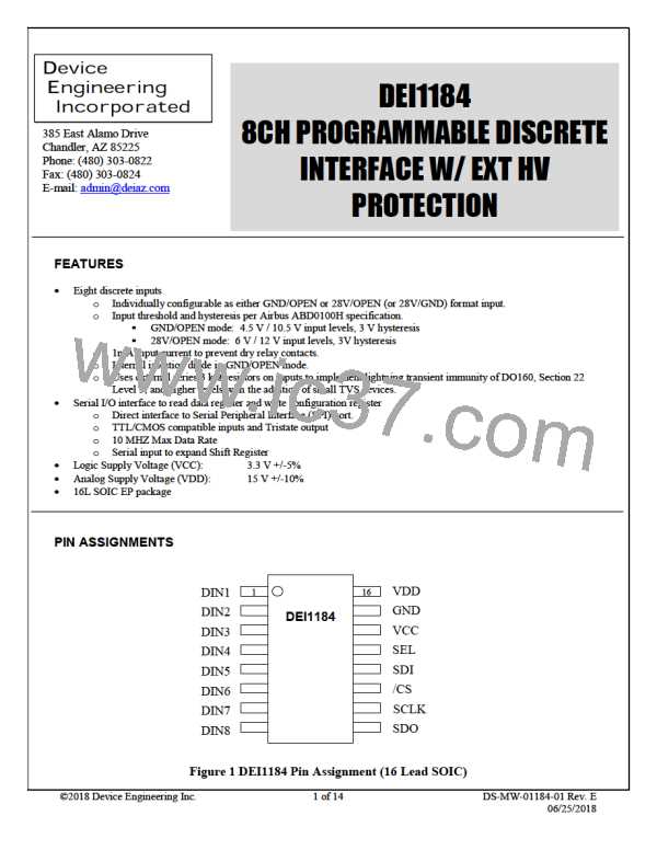
PACKAGE DESCRIPTION - 16L Narrow Body EP SOIC
Moisture Sensitivity:
Θja:
Level 1 / 260 ˚C per JEDEC J-STD-020
~40 ˚C/W (Mounted on 4 layer PCB with exposed pad soldered to PCB land with
thermal vias to internal GND plane)
~10 ˚C/W
Θjc:
Lead Finish:
Exposed Pad:
SnPb plated
Electrically Isolated from IC terminals.
The PCB design and layout is a significant factor in determining thermal resistance (Θja) of the IC package. Use maximum trace
width on all power and signal connections at the IC. These traces serve as heat spreaders which improve heat flow from the IC
leads. The exposed heat sink pad of the SOIC package should be soldered to a heat-spreader land pattern on the PCB. The IC
exposed pad is electrically isolated, so the PCB land may be at any potential, typically GND, for the best heat sink. Maximize
the PCB land size by extending it beyond the IC outline if possible. A grid of thermal VIAs, which drop down and connect to
the buried copper plane(s), should be placed under the heat-spreader land. A typical VIA grid is 12 mil holes on a 50 mil pitch.
The barrel is plated to about 1.0-ounce copper. Use as many VIAs as space allows. VIAs should be plugged to prevent voids
being formed between the exposed pad and PCB heat-spreader land due to solder escaping by the capillary effect. This can be
avoided by tenting the VIAs with solder mask.
Figure 15 16 Lead Narrow Body EP SOIC Outline Drawing
©2018 Device Engineering Inc.
13 of 14
DS-MW-01184-01 Rev. E
06/25/2018

 DEIAZ [ Device Engineering Incorporated ]