DS3251/DS3252/DS3253/DS3254
17. ELECTRICAL CHARACTERISTICS
ABSOLUTE MAXIMUM RATINGS
Voltage Range on Any Lead with Respect to VSS (except VDD)…………………………………………….-0.3V to +5.5V
Supply Voltage Range (VDD) with Respect to VSS…………………………………………………………..-0.3V to +3.63V
Ambient Operating Temperature Range……………………………………………………………………..-40°C to +85°C
Junction Operating Temperature Range……………………………………………………………………-40°C to +125°C
Storage Temperature Range………………………………………………………………………………...-55°C to +125°C
Soldering Temperature………………………………………………………….See IPC/JEDEC J-STD-020 Specification
Stresses beyond those listed under “Absolute Maximum Ratings” may cause permanent damage to the device. These are stress ratings only,
and functional operation of the device at these or any other conditions beyond those indicated in the operational sections of the specifications is
not implied. Exposure to the absolute maximum rating conditions for extended periods may affect device. Ambient operating temperature range
when device is mounted on a four-layer JEDEC test board with no airflow.
Note: The typical values listed in Tables 17-A through 17-J are not production tested.
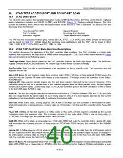
Table 17-A. Recommended DC Operating Conditions
(TA = -40°C to +85°C)
PARAMETER
Supply Voltage
Logic 1, All Other Input Pins
Logic 0, All Other Input Pins
SYMBOL
CONDITIONS
MIN
TYP
3.3
MAX
UNITS
VDD
VIH
VIL
3.135
2.0
-0.3
3.465
5.5
+0.8
V
V
V
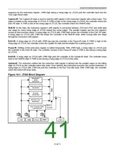
Table 17-B. DC Characteristics
(VDD = 3.3V M5%, TA = -40°C to +85°C.)
PARAMETER
SYMBOL
CONDITIONS
MIN
TYP
MAX
UNITS
DS3251
DS3252
DS3253
DS3254
DS3251
DS3252
80
150
220
290
60
120
200
280
360
100
160
Supply Current (Note 1)
IDD
mA
110
Supply Current, Transmitters Tri-Stated
IDDTTS
mA
(All TTSn Low) (Note 2)
DS3253
DS3254
160
210
220
280
Power-Down Current (All TPD, RPD
Control Bits High)
DS325x
(Note 2)
IDDPD
35
7
50
mA
pF
Lead Capacitance
CIO
IIL
10
Input Leakage, All Other Input Pins
Output Leakage (when High-Z)
Output Voltage (IO = -4.0mA)
Output Voltage (IO = +4.0mA)
(Note 3)
(Note 3)
-50
-10
2.4
0
+10
+10
VDD
0.4
ꢂA
ꢂA
V
ILO
VOH
VOL
V
Note 1:
TCLKn = STMCLK = 51.84MHz; TXPn/TXNn driving all ones into 75ꢀ resistive loads; analog loopback enabled; all other inputs
at VDD or grounded; all other outputs open.
Note 2:
Note 3:
TCLKn = STMCLK = 51.84MHz; other inputs at VDD or grounded; digital outputs left open circuited.
0V < VIN < VDD for all other digital inputs.
44 of 71

 DALLAS [ DALLAS SEMICONDUCTOR ]