DS3251/DS3252/DS3253/DS3254
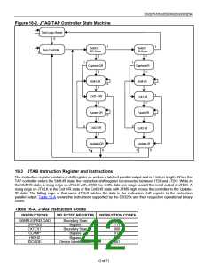
SAMPLE/PRELOAD. SAMPLE/RELOAD is a mandatory instruction for the IEEE 1149.1 specification. This
instruction supports two functions. The digital I/Os of the device can be sampled at the boundary scan register
without interfering with the device’s normal operation by using the Capture-DR state. SAMPLE/PRELOAD also
allows the DS325x to shift data into the boundary scan register through JTDI using the Shift-DR state.
EXTEST. EXTEST allows testing of the interconnections to the device. When the EXTEST instruction is latched in
the instruction register, the following actions occur. Once enabled through the Update-IR state, the parallel outputs
of the digital output pins are driven. The boundary scan register is connected between JTDI and JTDO. The
Capture-DR samples all digital inputs into the boundary scan register.
BYPASS. When the BYPASS instruction is latched into the parallel instruction register, JTDI connects to JTDO
through the 1-bit bypass test register. This allows data to pass from JTDI to JTDO without affecting the device’s
normal operation.
IDCODE. When the IDCODE instruction is latched into the parallel instruction register, the identification test
register is selected. The device identification code is loaded into the identification register on the rising edge of
JTCLK, following entry into the Capture-DR state. Shift-DR can be used to shift the identification code out serially
through JTDO. During Test-Logic-Reset, the identification code is forced into the instruction register’s parallel
output.
HIGHZ. All digital outputs are placed into a high-impedance state. The bypass register is connected between JTDI
and JTDO.
CLAMP. All digital output pins output data from the boundary scan parallel output while connecting the bypass
register between JTDI and JTDO. The outputs do not change during the CLAMP instruction.
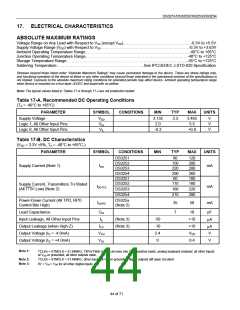
Table 16-B. JTAG ID Code
MANUFACTURER
PART
REVISION
DEVICE CODE
REQUIRED
CODE
DS3251
DS3252
DS3253
DS3254
Consult factory
Consult factory
Consult factory
Consult factory
0000000000101100
0000000000101101
0000000000101110
0000000000101111
00010100001
00010100001
00010100001
00010100001
1
1
1
1
16.4 JTAG Test Registers
IEEE 1149.1 requires a minimum of two test registers—the bypass register and the boundary scan register. An
optional test register, the identification register, has been included in the device design. It is used with the IDCODE
instruction and the Test-Logic-Reset state of the TAP controller.
Bypass Register. This is a single 1-bit shift register used with the BYPASS, CLAMP, and HIGHZ instructions,
which provide a short path between JTDI and JTDO.
Boundary Scan Register. This register contains a shift register path and a latched parallel output for control cells
and digital I/O cells. DS325x BSDL files are available at www.maxim-ic.com/TechSupport/telecom/bsdl.htm.
Identification Register. This register contains a 32-bit shift register and a 32-bit latched parallel output. It is
selected during the IDCODE instruction and when the TAP controller is in the Test-Logic-Reset state.
43 of 71

 DALLAS [ DALLAS SEMICONDUCTOR ]