DS3251/DS3252/DS3253/DS3254
LIST OF TABLES
Table 1-A. Applicable Telecommunications Standards............................................................................................... 6
Table 6-A. Global Pin Descriptions............................................................................................................................ 10
Table 6-B. Receiver Pin Descriptions........................................................................................................................ 11
Table 6-C. Transmitter Pin Descriptions.................................................................................................................... 11
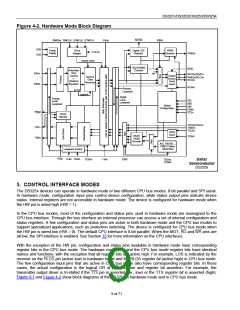
Table 6-D. Hardware Mode Pin Descriptions ............................................................................................................ 12
Table 6-E. Parallel Bus Mode Pin Descriptions......................................................................................................... 13
Table 6-F. SPI Bus Mode Pin Descriptions ............................................................................................................... 13
Table 6-G. Transmitter Data Select Options ............................................................................................................. 14
Table 6-H. Receiver PRBS Pattern Select Options................................................................................................... 14
Table 6-I. Hardware Mode Jitter Attenuator Configuration........................................................................................ 14
Table 7-A. Register Map............................................................................................................................................ 15
Table 9-A. DS3 Waveform Template......................................................................................................................... 29
Table 9-B. DS3 Waveform Test Parameters and Limits............................................................................................ 29
Table 9-C. STS-1 Waveform Template ..................................................................................................................... 29
Table 9-D. STS-1 Waveform Test Parameters and Limits........................................................................................ 29
Table 9-E. E3 Waveform Test Parameters and Limits .............................................................................................. 30
Table 14-A. Transformer Characteristics................................................................................................................... 36
Table 14-B. Recommended Transformers ................................................................................................................ 36
Table 16-A. JTAG Instruction Codes......................................................................................................................... 42
Table 16-B. JTAG ID Code........................................................................................................................................ 43
Table 17-A. Recommended DC Operating Conditions.............................................................................................. 44
Table 17-B. DC Characteristics ................................................................................................................................. 44
Table 17-C. Framer Interface Timing......................................................................................................................... 45
Table 17-D. Receiver Input Characteristics—DS3 and STS-1 Modes...................................................................... 47
Table 17-E. Receiver Input Characteristics—E3 Mode............................................................................................. 47
Table 17-F. Transmitter Output Characteristics—DS3 and STS-1 Modes................................................................ 48
Table 17-G. Transmitter Output Characteristics—E3 Mode...................................................................................... 48
Table 17-H. Parallel CPU Interface Timing ............................................................................................................... 49
Table 17-I. SPI Interface Timing................................................................................................................................ 54
Table 17-J. JTAG Interface Timing............................................................................................................................ 55
Table 18-A. Pin Assignments Sorted by Signal Name .............................................................................................. 56
Table 20-A. Thermal Properties, Natural Convection................................................................................................ 71
Table 20-B. Theta-JA (ꢁ ) vs. Airflow....................................................................................................................... 71
JA
4 of 71

 DALLAS [ DALLAS SEMICONDUCTOR ]