DS3251/DS3252/DS3253/DS3254
LIST OF FIGURES
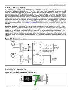
Figure 2-1. External Connections ................................................................................................................................ 7
Figure 3-1. 4-Port Unchannelized DS3/E3 Card ......................................................................................................... 7
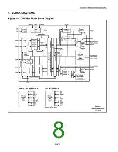
Figure 4-1. CPU Bus Mode Block Diagram ................................................................................................................. 8
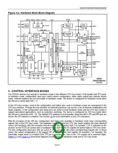
Figure 4-2. Hardware Mode Block Diagram ................................................................................................................ 9
Figure 7-1. Status Register Logic .............................................................................................................................. 16
Figure 8-1. Receiver Jitter Tolerance ........................................................................................................................ 27
Figure 9-1. E3 Waveform Template........................................................................................................................... 30
Figure 9-2. DS3 AIS Structure................................................................................................................................... 31
Figure 10-1. Jitter Attenuation/Jitter Transfer............................................................................................................ 33
Figure 11-1. PRBS Output with Normal RCLK Operation ......................................................................................... 34
Figure 11-2. PRBS Output with Inverted RCLK Operation........................................................................................ 34
Figure 15-1. SPI Clock Polarity and Phase Options.................................................................................................. 38
Figure 15-2. SPI Bus Transactions............................................................................................................................ 39
Figure 16-1. JTAG Block Diagram............................................................................................................................. 41
Figure 16-2. JTAG TAP Controller State Machine .................................................................................................... 42
Figure 17-1. Transmitter Framer Interface Timing Diagram...................................................................................... 46
Figure 17-2. Receiver Framer Interface Timing Diagram.......................................................................................... 46
Figure 17-3. Parallel CPU Interface Timing Diagram (Nonmultiplexed).................................................................... 50
Figure 17-4. Parallel CPU Interface Timing Diagram (Multiplexed) .......................................................................... 52
Figure 17-5. SPI Interface Timing Diagram ............................................................................................................... 54
Figure 17-6. JTAG Timing Diagram........................................................................................................................... 55
Figure 18-1. DS3251 Hardware Mode Pin Assignment............................................................................................. 58
Figure 18-2. DS3251 Parallel Bus Mode Pin Assignment......................................................................................... 59
Figure 18-3. DS3251 SPI Bus Mode Pin Assignment ............................................................................................... 60
Figure 18-4. DS3252 Hardware Mode Pin Assignment............................................................................................. 61
Figure 18-5. DS3252 Parallel Bus Mode Pin Assignment......................................................................................... 62
Figure 18-6. DS3252 SPI Bus Mode Pin Assignment ............................................................................................... 63
Figure 18-7. DS3253 Hardware Mode Pin Assignment............................................................................................. 64
Figure 18-8. DS3253 Parallel Bus Mode Pin Assignment......................................................................................... 65
Figure 18-9. DS3253 SPI Bus Mode Pin Assignment ............................................................................................... 66
Figure 18-10. DS3254 Hardware Mode Pin Assignment........................................................................................... 67
Figure 18-11. DS3254 Parallel Bus Mode Pin Assignment....................................................................................... 68
Figure 18-12. DS3254 SPI Bus Mode Pin Assignment ............................................................................................. 69
3 of 71

 DALLAS [ DALLAS SEMICONDUCTOR ]