DS2406
Status Memory location 7 serves three purposes: 1) it holds the selection code for the Conditional Search
function, 2) provides the bus master a memory mapped access to the channel flip-flops that control the
PIO output transistors, and 3) allows the bus master to determine whether the device is hooked up to a
VCC power supply. Bit locations 0 to 4 store the conditional search settings. Their codes are explained in
the section “ROM Function Commands” later in this document. The channel flip-flops are accessible
through bit locations 5 and 6 as well as through the Channel Access function. The power-on default for
the conditional search settings and the channel flip-flops is all 1’s. Setting a channel flip-flop to 0 will
make the associated PIO-transistor conducting or on; setting the flip-flop to 1 will switch the transistor
off, which is identical to the power-on default. With the VCC pin connected to a suitable power supply the
power indicator bit 7 will read 1. The power supply indicator can also be read through the Channel
Access function.
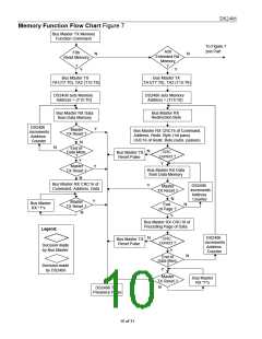
MEMORY FUNCTION COMMANDS
The “Memory Function Flow Chart” (Figure 7) describes the protocols necessary for accessing the
various data fields and PIO channels within the DS2406. The Memory Function Control section, 8-bit
scratchpad, and the Program Voltage Detect circuit combine to interpret the commands issued by the bus
master and create the correct control signals within the device. A three-byte protocol is issued by the bus
master. It is comprised of a command byte to determine the type of operation and two address bytes to
determine the specific starting byte location within a data field or to supply and exchange setup and status
data when accessing the PIO channels. The command byte indicates if the device is to be read or written
or if the PIO channels are to be accessed. Writing data involves not only issuing the correct command
sequence but also providing a 12-volt programming voltage at the appropriate times. To execute a write
sequence, a byte of data is first loaded into the scratchpad and then programmed into the selected address.
Write sequences always occur a byte at a time. To execute a read sequence, the starting address is issued
by the bus master and data is read from the part beginning at that initial location and continuing to the end
of the selected data field or until a reset sequence is issued. All bits transferred to the DS2406 and
received back by the bus master are sent least significant bit first.
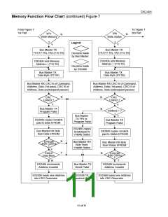
Read Memory [F0h]
The Read Memory command is used to read data from the 1024-bit EPROM data memory field. The bus
master follows the command byte with a two-byte address (TA1=(T7:T0), TA2=(T15:T8)) that indicates
a starting byte location within the data field. Since the data memory contains 128 bytes, T15:T8 and T7
should all be zero. With every subsequent read data time slot the bus master receives data from the
DS2406 starting at the initial address and continuing until the end of the 1024-bits data field is reached or
until a Reset Pulse is issued. If reading occurs through the end of memory space, the bus master may
issue sixteen additional read time slots and the DS2406 will respond with a 16-bit CRC of the command,
address bytes and all data bytes read from the initial starting byte through the last byte of memory. This
CRC is the result of clearing the CRC generator and then shifting in the command byte followed by the
two address bytes and the data bytes beginning at the first addressed memory location and continuing
through to the last byte of the EPROM data memory. After the CRC is received by the bus master, any
subsequent read time slots will appear as logical 1s until a Reset Pulse is issued. Any reads ended by a
Reset Pulse prior to reaching the end of memory will not have the 16-bit CRC available.
Typically the software controlling the device should store a 16-bit CRC with each page of data to insure
rapid, error-free data transfers that eliminate having to read a page multiple times to determine if the
received data is correct or not. (See Application Note 114 for the recommended file structure). If CRC
values are imbedded within the data it is unnecessary to read the end-of-memory CRC. The Read
Memory command can be ended at any point by issuing a Reset Pulse.
7 of 31

 DALLAS [ DALLAS SEMICONDUCTOR ]