DS2406
MEMORY MAP
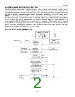
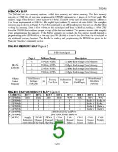
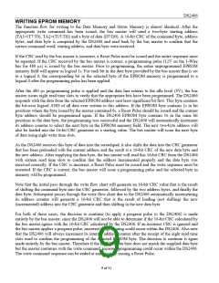
The DS2406 has two memory sections, called data memory and status memory. The data memory
consists of 1024 bits of one-time programmable EPROM organized as 4 pages of 32 bytes each. The
address range of the device’s status memory is 8 bytes. The first seven bytes of status memory (addresses
0 to 6) are implemented as EPROM. The eighth byte (address 7) consists of static RAM. The complete
memory map is shown in Figure 5. The 8-bit scratchpad is an additional register that acts as a buffer when
writing the memory. Data is first written to the scratchpad and then verified by reading a 16-bit CRC
from the DS2406 that confirms proper receipt of the data and address. This process ensures data integrity
when programming the memory. If the buffer contents are correct, the bus master should transmit a
programming pulse (EPROM) or a dummy byte FFh (RAM) to transfer the data from the scratchpad to
the addressed memory location. The details for reading and programming the DS2406 are given in the
Memory Function Commands section.
DS2406 MEMORY MAP Figure 5
8-Bit Scratchpad
Page #
Address Range
0000h to 001Fh
0020h to 003Fh
0040h to 005Fh
0060h to 007Fh
Description
0
1
2
3
32-Byte final storage Data Memory
32-Byte final storage Data Memory
32-Byte final storage Data Memory
32-Byte final storage Data Memory
1K-Bit
EPROM
Valid Device
Settings
Write-Protect
8 Bytes
Status
Memory
Factory
Test Byte
Redirection
Bytes
Bitmap of
Used Pages
Bits Data
Memory
00
(SRAM)
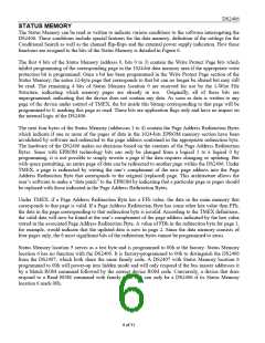
DS2406 STATUS MEMORY MAP Figure 6
ADDRESS
0 (EPROM)
1 (EPROM)
2 (EPROM)
3 (EPROM)
4 (EPROM)
5 (EPROM)
6 (EPROM)
7 (SRAM)
BIT 7
BIT 6
BIT 5
BIT 4
BIT 3
WP3
BIT 2
WP2
BIT 1
WP1
Redir. 0 Redir. 0
Redir. 1 Redir. 1
Redir 2
Redir 3
BIT 0
WP0
BM3
BM2
BM1
BM0
1
1
1
1
1
1
1
1
1
1
1
1
1
1
1
1
1
1
1
1
1
1
1
1
Redir 2
Redir 3
EPROM Factory Test byte
Don’t care, always reads 00
PIO-A CSS4 CSS3
Supply
PIO-B
CSS2
CSS1
Source
Select
CSS0
Polarity
Indication Channel Channel Channel Channel Source
(read only) Flip-flop Flip-flop Select
Select
Select
5 of 31

 DALLAS [ DALLAS SEMICONDUCTOR ]