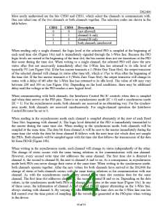
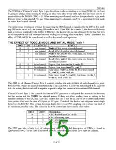
DS2406
Write Memory [0Fh]
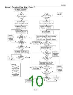
The Write Memory command is used to program the 1024-bit EPROM data memory. The details of the
functional flow chart are described in the section “Writing EPROM Memory”. The data memory address
range is 0000h to 007Fh. If the bus master sends a starting address higher than this, the nine most
significant address bits are set to zeros by the internal circuitry of the chip. This will result in a mismatch
between the CRC calculated by the DS2406 and the CRC calculated by the bus master, indicating an error
condition.
Write Status [55h]
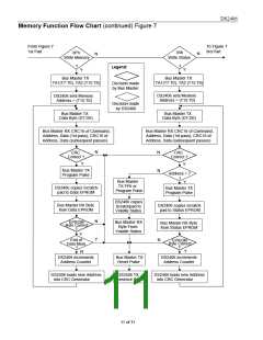
The Write Status command is used to program the Status Memory, which includes the specification of the
Conditional Search Settings. The details of the functional flow chart are described in the section “Writing
EPROM Memory”.
The Status Memory address range is 0000h to 0007h. The general programming algorithm is valid for the
EPROM section of the Status Memory (addresses 0 to 4) only. The Status memory locations 5 and 6 are
already pre-programmed to 00h and therefore cannot be altered. Status memory location 7 consists of
static RAM, which can be reprogrammed without limitation and does not require a 12V programming
pulse. The supply indication (bit 7) is read-only; attempts to write to it are ignored. The function flow for
writing to status memory location 7 is basically the same as for the other EPROM Status Memory Bytes.
However, instead of a programming pulse the bus master may send a FFh byte (equivalent to 8 Write-One
Time Slots) to transfer the new value from the scratchpad to the status memory.
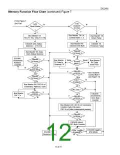
If the bus master sends a starting address higher than 0007h, the nine most significant address bits are set
to zeros by the internal circuitry of the chip. The address bits T3:T6 remain unchanged and will be
ignored by the address decoder of the DS2406. Only if one or more of the address bits T8:T15 is set, the
bus master will be able to discover an error condition based on the CRC16 that is calculated by the
DS2406.
Read Status [AAh]
The Read Status command is used to read data from the Status Memory field. The functional flow chart
of this command is identical to the Read Memory command. Since the Status Memory is only 8 bytes, the
DS2406 will send the 16-bit CRC after the last byte of status information has been transmitted.
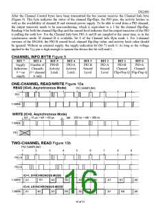
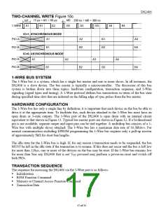
Channel Access [F5h]
The Channel Access command is used to access the PIO channels to sense the logical status of the output
node and the output transistor and to change the status of the output transistor. The bus master will follow
the command byte with two Channel Control Bytes and will receive back the Channel Info byte. The
Channel Control bytes allow the master to select a PIO-channel to communicate with, to specify
communication parameters, and to reset the activity latches. Figure 8 shows the details Channel Control
Byte 1. The bit assignments of Channel Control Byte 2 are reserved for future development. The bus
master should always send FFh for the second Channel Control Byte.
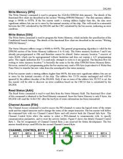
CHANNEL CONTROL BYTE 1 Figure 8
BIT 7
BIT 6
BIT 5
BIT 4
BIT 3
BIT 2
BIT 1
BIT 0
ALR
IM
TOG
IC
CHS1
CHS0
CRC1
CRC0
13 of 31

 DALLAS [ DALLAS SEMICONDUCTOR ]