DS1050/DS1052
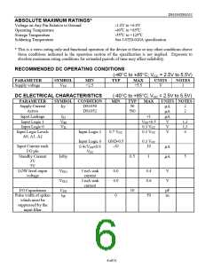
ABSOLUTE MAXIMUM RATINGS*
Voltage on Any Pin Relative to Ground
Operating Temperature
-1.0V to +6.0V
-40oC to +85oC
Storage Temperature
-55oC to +125oC
Soldering Temperature
See J-STD-020A specification
* This is a stress rating only and functional operation of the device at these or any other conditions above
those conditions indicated in the operation section of the specification is not implied. Exposure to
absolute maximum rating conditions for extended periods of time may affect reliability.
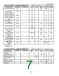
RECOMMENDED DC OPERATING CONDITIONS
(-40°C to +85°C; VCC = 2.5V to 5.5V)
PARAMETER
SYMBOL
MIN
TYP
MAX
UNITS
NOTES
Supply voltage
VCC
+2.5
+5.5
V
1
DC ELECTRICAL CHARACTERISTICS
(-40°C to +85°C; VCC = 2.5V to 5.5V)
PARAMETER
Supply Current
Active
SYMBOL CONDITION
MIN
TYP
50
500
MAX
UNITS NOTES
ICC
DS1050
DS1052
2
2
µA
µA
µA
V
V
V
Input Leakage
Input Logic 1
Input Logic 0
Input Logic Levels
A0, A1, A2
ILI
VIH
VIL
+1
VCC+0.5
0.3 VCC
0.3 VCC
1,3
1,3
4
Input Logic 1
0.7 VCC
Input Logic 0
0.4<VI/O<0.9
VCC
GND-0.5
-10
0.3 VCC
10
Input Current each
I/O pin
Standby Current
3V
µA
µA
Istby
0.5
10
1
5
5V
LOW level ouput
voltage
VOL1
VOL2
3 mA sink
current
3 mA sink
current
0.0
0.0
0.4
0.6
V
V
I/O Capacitance
Pulse width of spikes
which must be
CI/O
tSP
pF
ns
0
50
suppressed by the
input filter
6 of 11

 DALLAS [ DALLAS SEMICONDUCTOR ]