DS1050/DS1052
NOTES:
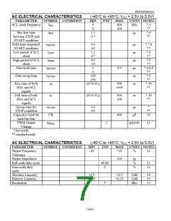
1. All voltages are referenced to ground.
2. ISTBY specified for VCC between 3.0V and 5.0V. control port logic pins are driven to the appropriate
logic levels. Appropriate logic levels specify that logic inputs are within a 0.5V of ground or VCC for
the corresponding inactive state.
3. I/O pins of fast mode devices must not obstruct the SDA and SCL lines if VCC is switched off.
4. Address Inputs, A0, A1, and A2, should be tied to either VCC or GND depending on the desired
address selections.
5.
ISTBY specified for VCC between 3.0V and 5.0V, control port logic pins are driven to the appropriate
logic levels.
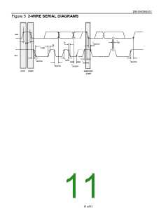
6. A fast mode device can be used in a standard mode system, but the requirement tSU:DAT > 250 ns
must then be met. This will automatically be the case if the device does not stretch the LOW period
of the SCL signal. If such a device does stretch the LOW period of the SCL signal, it must output
the next data bit to the SDA line tRMAX + tSU:DAT = 1000+250=1250 ns before the SCL line is
released.
7. After this period, the first clock pulse is generated.
8. The maximum tSU:DAT has only to be met if the device does not stretch the LOW period (tLOW) of the
SCL signal.
9. A device must internally provide a hold time of at least 300 ns for the SDA signal (referred to the
V
IH MIN of the SCL signal) in order to bridge the undefined region of the falling edge of SCL.
10. CB - total capacitance of one bus line in picofarads, timing referenced to (0.9)(VCC) and (0.1)(VCC).
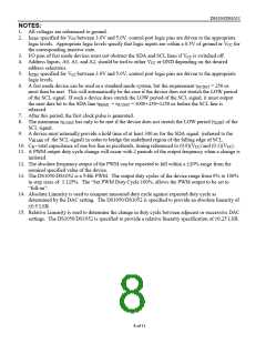
11. A PWM output duty cycle change will occur with 2 periods of the output frequency when a change is
initiated.
12. The absolute frequency output of the PWM can be expected to fall within a ±20% range from the
nominal specified value of the device.
13. The DS1050/DS1052 is a 5-Bit PWM. The output duty cycles of the device range from 0% to 100%
in step sizes of 3.125%. The “Set PWM Duty Cycle 100%, allows the PWM output to be set to
“full-on”.
14. Absolute Linearity is used to compare measured duty cycle against expected duty cycle as
determined by the DAC setting. The DS1050/DS1052 is specified to provide an absolute linearity of
±0.5 LSB.
15. Relative Linearity is used to determine the change in duty cycle between adjacent or successive DAC
settings. The DS1050/DS1052 is specified to provide a relative linearity specification of ±0.25 LSB.
8 of 11

 DALLAS [ DALLAS SEMICONDUCTOR ]