63
8Bit Single Chip Microcontroller
DMC73C168
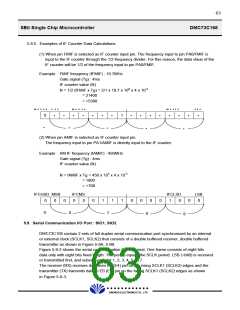
5.8.5. Examples of IF Counter Data Calculations
(1) When pin FMIF is selected as IF counter input pin. The frequency input to pin PA0/FMIF is
input to the IF counter through the 1/2 frequency divider. For this reason, the data vlaue of the
IF counter will be 1/2 of the frequency input to pin PA0/FMIF.
Example : FMIF freuqency (fFMIF) : 10.7MHz
Gate signal (Tg) : 4ms
IF counter value (N)
N = 1/2 (fFMIF x Tg) = 2/1 x 10.7 x 106 x 4 x 10-3
= 21400
= >5398
IFCHSD MSB
IFCMSD
IFCLSD
LSB
0
0
1
0
1
0
1
0
0
1
1
0
0
1
1
0
0
0
5
3
9
8
(2) When pin AMIF is selected as IF counter input pin.
The frequency input to pin PA1/AMIF is directly input to the IF counter.
Example : AM IF frequency (fAMIF) : 450MHz
Gate signal (Tg) : 4ms
IF counter value (N)
N = fAMIF x Tg = 450 x 103 x 4 x 10-3
= 1800
= >708
IFCHSD MSB
IFCMS
IFCLSD
LSB
0
0
0
0
0
0
0
1
1
1
0
0
0
0
1
0
0
0
0
7
0
8
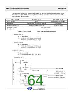
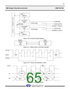
5.9. Serial Communication I/O Port : SIO1, SIO2
DMC73C168 contain 2 sets of full duplex serial communication port synchronized by an internal
or external clock (SCLK1, SCLK2) that consists of a double buffered receiver, double buffered
transmitter as shown in Figure 5-9A, 5-9B.
Figure 5-9-2 shows the serial communication frame format. One frame consists of eight bits
data only with eight bits fixed length. The period equals the SCLK period. LSB (=bit0) is received
or transmitted first, and subsequently bit 1, 2, 3, 4, 5, 6, 7.
The receiver (RX) receives data from E1 (E4) pin on the rising SCLK1 (SCLK2) edges and the
transmitter (TX) transmits data to E0 (E3) pin on the falling SCLK1 (SCLK2) edges as shown
in Figure 5-9-3.
£Ä£Á£Å£×£Ï £Ï
DAEWOO ELECTRONICS CO., LTD.

 DAEWOO [ DAEWOO Electronic Components ]