SL811HS
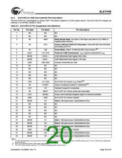
Table 6-2. SL811HST-AC Pin Assignments and Definitions (continued)
Pin No.
33
Pin Type
BIDIR
NC
Pin Name
D6
Pin Description
Data 6. Microprocessor Data/(Address) Bus.
34
NC
NC
35
NC
NC
NC
36
NC
NC
NC
37
NC
NC
NC
38
NC
NC
NC
39
BIDIR
IN
D7
Data 7. Microprocessor Data/(Address) Bus.
40
M/S
Master/Slave Mode Select. “1” selects Slave. “0” = Master.
41
VDD
IN
+3.3 VDC
A0
SL811HST-AC Device VDD Power.
42
A0 = “0.” Selects address pointer. Reg.A0 = “1.” Selects data buffer or
register.[12]
43
44
45
IN
OUT
IN
nDACK
nDRQ
NRD
DMA Acknowledge. An active LOW input used to interface to an
external DMA controller. DMA is enabled only in slave mode. In host
mode, pin should be tied HIGH (logic “1”) .
DMA Request. An active LOW output used with an external DMA
controller. nDRQ and nDACK form the handshake for DMA data
transfers. In host mode, pin must be left unconnected .
Read Strobe Input. An active LOW input used with nCS to Read
registers/data memory.
46
47
48
NC
NC
NC
NC
NC
NC
NC
NC
NC
Notes:
12. The A0 Address bit is used to access address register or data registers in I/O Mapped or Memory Mapped applications.
6.2.4
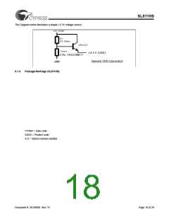
Package Markings (SL811HST-AC)
SL811HST
YYWW-X.X
XXXX
YYWW = Date code
XXXX = Product code
X.X = Silicon revision number
Document #: 38-08008 Rev. *A
Page 21 of 29

 CYPRESS [ CYPRESS ]