SL811HS
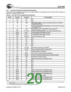
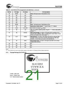
6.2.3
SL811HST-AC USB Host Controller Pins Description
The SL811HST-AC is packaged in a 48-pin TQFP. The device requires a 3.3VDC power source. The SL811HST-AC requires an
external 12 or 48 MHz crystal or Clock.
Table 6-2. SL811HST-AC Pin Assignments and Definitions
Pin No.
Pin Type
NC
Pin Name
NC
Pin Description
1
2
3
NC
NC
NC
NC
IN
nWR
Write Strobe Input. An active LOW input used with nCS to Write to
registers/data memory.
4
IN
nCS
Active LOW SL811HST-AC Chip select. Used with nRD and nWr when
accessing SL811HT.
5
IN
VDD1
BIDIR
BIDIR
GND
NC
CM
+3.3 VDC
DATA +
DATA -
USB GND
NC
Clock Mode. Select 12-MHz/48-MHz Clock Source.[9]
6
Power for USB Transceivers. VDD1 may be connected to VDD.
7
USB Differential Data Signal HIGH Side
8
USB Differential Data Signal LOW Side
9
Ground Connection for USB
10
11
12
13
14
15
16
17
18
19
20
21
22
23
24
25
26
27
28
29
30
31
32
NC
NC
NC
NC
NC
NC
NC
NC
NC
NC
NC
NC
NC
VDD
IN
+3.3 VDC
CLK/X1
X2
SL811HST-AC Device VDD Power[10]
Clock or External Crystal X1 connection[11]
External Crystal X2 connection
SL811HST-AC Device active low reset input
Active HIGH Interrupt Request output to external controller
SL811HST-AC Device Ground
Data 0. Microprocessor Data/(Address) Bus.
NC
OUT
IN
NRST
INTRQ
GND
D0
OUT
GND
BIDIR
NC
NC
NC
NC
NC
NC
NC
NC
NC
NC
NC
NC
NC
NC
BIDIR
BIDIR
BIDIR
GND
BIDIR
BIDIR
D1
Data 1. Microprocessor Data/(Address) Bus.
Data 2. Microprocessor Data/(Address) Bus.
Data 3. Microprocessor Data/(Address) Bus.
SL811HST-AC Device Ground
Data 4. Microprocessor Data/(Address) Bus.
Data 5. Microprocessor Data/(Address) Bus.
D2
D3
GND
D4
D5
Notes:
9. The CM Clock Multiplier pin should be tied HIGH for a 12-MHz clock source and tied to ground for a 48-MHz clock source. In SL11H, this pin was designated
as ALE input pin.
10. VDD can be derived from the USB supply. See diagram.
11. The X1/X2 Clock requires external 12- or 48-MHz matching crystal or clock source.
Document #: 38-08008 Rev. *A
Page 20 of 29

 CYPRESS [ CYPRESS ]