CY8C9520A, CY8C9540A
CY8C9560A
AC Electrical Characteristics
AC General Purpose IO Specifications
Table 25 lists guaranteed maximum and minimum specifications for the voltage and temperature ranges: 4.75V to 5.25V and -40°C
≤ TA ≤ 85°C, or 3.0V to 3.6V and -40°C ≤ TA ≤ 85°C, respectively. Typical parameters apply to 5V and 3.3V at 25°C and are for design
guidance only or unless otherwise specified.
Table 25. AC GPIO Specifications
Symbol
FGPIO
Description
Min
Typ
Max
12
Units
MHz
ns
Notes
GPIO Operating Frequency
0
3
2
–
–
–
Normal Strong Mode
TRiseF
TFallF
Rise time, normal strong mode, Cload = 50 pF
Fall time, normal strong mode, Cload = 50 pF
Rise time, slow strong mode, Cload = 50 pF
Fall time, slow strong mode, Cload = 50 pF
18
18
–
Vdd = 4.75 to 5.25V, 10% - 90%
Vdd = 4.75 to 5.25V, 10% - 90%
Vdd = 3 to 5.25V, 10% - 90%
Vdd = 3 to 5.25V, 10% - 90%
ns
TRiseS
TFallS
10
10
27
22
ns
–
ns
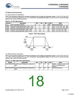
Figure 8. GPIO Timing Diagram
90%
GPIO
Pin
Output
Voltage
10%
TRiseF
TRiseS
TFallF
TFallS
AC PWM Output Jitter Specifications
Table 26 lists guaranteed maximum and minimum specifications for the voltage and temperature ranges: 4.75V to 5.25V and -40°C
≤ TA ≤ 85°C, or 3.0V to 3.6V and -40°C ≤ TA ≤ 85°C, respectively. Typical parameters apply to 5V and 3.3V at 25°C and are for design
guidance only or unless otherwise specified.
Table 26. AC PWM Output Jitter Specifications
Symbol
Description
Min
Typ
0.1
Max
1.5
Units
Notes
Jitter24MHzPWM 24MHzbasedPWMpeak-to-peakperiod –
jitter
%
24 MHz, 1.5 MHz, 93.75 kHz and
367.6 Hz (programmable)
sources.
Jitter32kHzPWM 32 kHz-based PWM peak-to-peak period –
jitter
2.5
5.0
%
32 kHz clock source.
Document Number: 38-12036 Rev. *B
Page 18 of 24
[+] Feedback

 CYPRESS [ CYPRESS ]