CY8C21x34 Final Data Sheet
3. Electrical Specifications
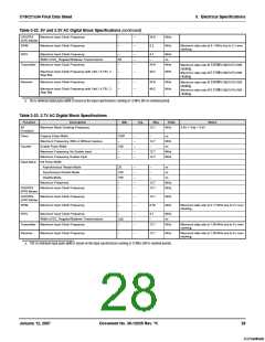
Table 3-22. 5V and 3.3V AC Digital Block Specifications (continued)
CRCPRS
(CRC Mode)
Maximum Input Clock Frequency
–
–
24.6
8.2
MHz
MHz
SPIM
Maximum Input Clock Frequency
–
–
Maximum data rate at 4.1 MHz due to 2 x over
clocking.
SPIS
Maximum Input Clock Frequency
–
–
–
–
4.1
–
MHz
ns
Width of SS_ Negated Between Transmissions
50
–
Transmitter Maximum Input Clock Frequency
24.6
MHz
Maximum data rate at 3.08 MHz due to 8 x over
clocking.
Maximum Input Clock Frequency with Vdd ≥ 4.75V, 2
Stop Bits
–
–
49.2
MHz
Maximum data rate at 6.15 MHz due to 8 x over
clocking.
Receiver
Maximum Input Clock Frequency
–
–
–
–
24.6
49.2
MHz
MHz
Maximum data rate at 3.08 MHz due to 8 x over
clocking.
Maximum data rate at 6.15 MHz due to 8 x over
clocking.
Maximum Input Clock Frequency with Vdd ≥ 4.75V, 2
Stop Bits
a. 50 ns minimum input pulse width is based on the input synchronizers running at 12 MHz (84 ns nominal period).
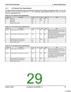
Table 3-23. 2.7V AC Digital Block Specifications
Function
Description
Min
Typ
Max
12.7
Units
MHz
Notes
All
Maximum Block Clocking Frequency
2.4V < Vdd < 3.0V.
Functions
Timer
a
Capture Pulse Width
–
–
–
–
–
–
ns
100
Maximum Frequency, With or Without Capture
Enable Pulse Width
–
12.7
–
MHz
ns
Counter
100
–
Maximum Frequency, No Enable Input
Maximum Frequency, Enable Input
12.7
12.7
MHz
MHz
–
Dead Band Kill Pulse Width:
Asynchronous Restart Mode
20
100
100
–
–
–
–
–
–
–
ns
Synchronous Restart Mode
Disable Mode
–
ns
–
ns
Maximum Frequency
12.7
12.7
MHz
MHz
CRCPRS
Maximum Input Clock Frequency
–
(PRS Mode)
CRCPRS
(CRC Mode)
Maximum Input Clock Frequency
Maximum Input Clock Frequency
–
–
–
–
12.7
6.35
MHz
MHz
SPIM
Maximum data rate at 3.17 MHz due to 2 x over
clocking.
SPIS
Maximum Input Clock Frequency
–
–
–
–
4.1
–
MHz
ns
Width of SS_ Negated Between Transmissions
100
–
Transmitter Maximum Input Clock Frequency
12.7
MHz
Maximum data rate at 1.59 MHz due to 8 x over
clocking.
Receiver Maximum Input Clock Frequency
–
–
12.7
MHz
Maximum data rate at 1.59 MHz due to 8 x over
clocking.
a. 100 ns minimum input pulse width is based on the input synchronizers running at 12 MHz (84 ns nominal period).
January 12, 2007
Document No. 38-12025 Rev. *K
28
[+] Feedback

 CYPRESS [ CYPRESS ]