CY8C21x34 Final Data Sheet
3. Electrical Specifications
2
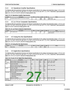
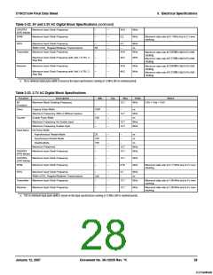
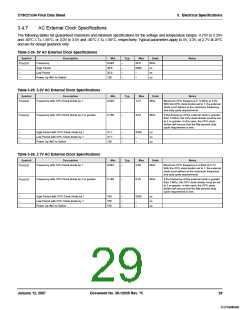
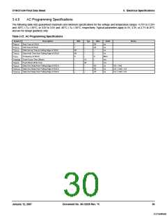
3.4.9
AC I C Specifications
The following tables list guaranteed maximum and minimum specifications for the voltage and temperature ranges: 4.75V to 5.25V
and -40°C ≤ TA ≤ 85°C, 3.0V to 3.6V and -40°C ≤ TA ≤ 85°C, or 2.4V to 3.0V and -40°C ≤ TA ≤ 85°C, respectively. Typical parameters
apply to 5V, 3.3V, or 2.7V at 25°C and are for design guidance only.
Table 3-28. AC Characteristics of the I2C SDA and SCL Pins for Vdd ≥ 3.0V
Standard Mode
Min Max
100
Fast Mode
Min Max
Symbol
SCLI2C
Description
SCL Clock Frequency
Units
kHz
Notes
F
T
0
0
400
–
Hold Time (repeated) START Condition. After this
period, the first clock pulse is generated.
4.0
–
0.6
µs
HDSTAI2C
T
T
T
T
T
T
T
T
LOW Period of the SCL Clock
HIGH Period of the SCL Clock
Set-up Time for a Repeated START Condition
Data Hold Time
4.7
4.0
4.7
0
–
–
–
–
–
–
–
–
1.3
0.6
0.6
0
–
µs
µs
µs
µs
ns
µs
µs
ns
LOWI2C
–
HIGHI2C
SUSTAI2C
HDDATI2C
SUDATI2C
SUSTOI2C
BUFI2C
–
–
a
Data Set-up Time
250
4.0
–
100
0.6
1.3
0
Set-up Time for STOP Condition
–
Bus Free Time Between a STOP and START Condition 4.7
–
Pulse Width of spikes are suppressed by the input fil-
ter.
–
50
SPI2C
a. A Fast-Mode I2C-bus device can be used in a Standard-Mode I2C-bus system, but the requirement tSU;DAT ≥ 250 ns must then be met. This will automatically be
the case if the device does not stretch the LOW period of the SCL signal. If such device does stretch the LOW period of the SCL signal, it must output the next data
bit to the SDA line trmax + tSU;DAT = 1000 + 250 = 1250 ns (according to the Standard-Mode I2C-bus specification) before the SCL line is released.
Table 3-29. 2.7V AC Characteristics of the I2C SDA and SCL Pins (Fast Mode not Supported)
Standard Mode
Min Max
100
Fast Mode
Min Max
Symbol
SCLI2C
Description
SCL Clock Frequency
Units
kHz
Notes
F
T
0
–
–
–
–
Hold Time (repeated) START Condition. After this
period, the first clock pulse is generated.
4.0
–
µs
HDSTAI2C
T
T
T
T
T
T
T
T
LOW Period of the SCL Clock
HIGH Period of the SCL Clock
Set-up Time for a Repeated START Condition
Data Hold Time
4.7
4.0
4.7
0
–
–
–
–
–
–
–
–
–
–
–
–
–
–
–
–
–
–
–
–
–
–
–
–
µs
µs
µs
µs
ns
µs
µs
ns
LOWI2C
HIGHI2C
SUSTAI2C
HDDATI2C
SUDATI2C
SUSTOI2C
BUFI2C
Data Set-up Time
250
4.0
Set-up Time for STOP Condition
Bus Free Time Between a STOP and START Condition 4.7
Pulse Width of spikes are suppressed by the input fil-
ter.
–
SPI2C
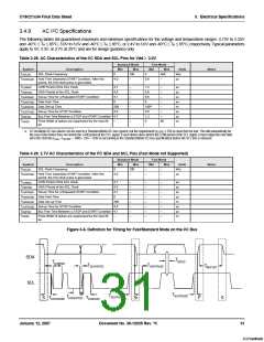
Figure 3-6. Definition for Timing for Fast/Standard Mode on the I2C Bus
SDA
SCL
TSPI2C
T
LOWI2C
TSUDATI2C
THDSTAI2C
TBUFI2C
TSUSTOI2C
TSUSTAI2C
THDDATI2C
THDSTAI2C
THIGHI2C
S
Sr
P
S
January 12, 2007
Document No. 38-12025 Rev. *K
31
[+] Feedback

 CYPRESS [ CYPRESS ]