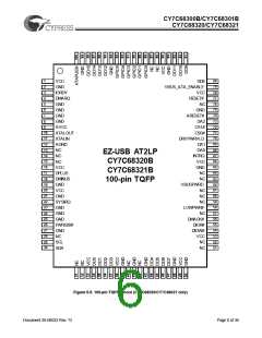
CY7C68300B/CY7C68301B
CY7C68320/CY7C68321
resonant fundamental mode) crystal is used, but a 24-MHz
square wave from another source can also be used. If a crystal
is used, connect its pins to XTALIN and XTALOUT, and also
through 12-pF capacitors to GND as shown in Figure 5-6. If an
alternate clock source is used, apply it to XTALIN and leave
XTALOUT open.
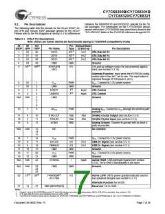
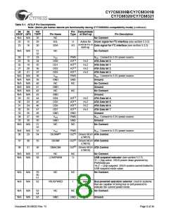
5.3
Additional Pin Descriptions
5.3.1
DPLUS, DMINUS
DPLUS and DMINUS are the USB signaling pins; they should
be tied to the D+ and D– pins of the USB connector. Because
they operate at high frequencies, the USB signals require
special consideration when designing the layout of the PCB.
See section 15.0 for PCB layout recommendations. When
RESET# is released, the internal pull-up on D+ is controlled
by VBUS_ATA_ENABLE. When VBUS_ATA_ENABLE is
HIGH, D+ is pulled up.
5.3.4
SYSIRQ
The SYSIRQ pin provides a way for systems to request service
from host software by using the USB Interrupt pipe. If the
AT2LP has no pending interrupt data to return, USB interrupt
pipe data requests are NAKed. If pending data is available, the
AT2LP returns 16 bits of data; this data indicates the
HS_MODE signal (that indicates whether AT2LP is operating
in high-speed or full-speed), the VBUSPWRD pin, and the
GPIO pins. Table 5-2 gives the bitmap for the data returned on
the interrupt pipe and Figure 5-7 depicts the latching algorithm
incorporated by AT2LP.
5.3.2
SCL, SDA
The clock and data pins for the I2C port should be connected
to the configuration EEPROM and to 2.2K pull-up resistors tied
to VCC. The SCL and SDA pins are active for several milli-
seconds at start-up.
The SYSIRQ pin must be tied low if the HID function is used
(refer to Section 6.0).
5.3.3
XTALIN, XTALOUT
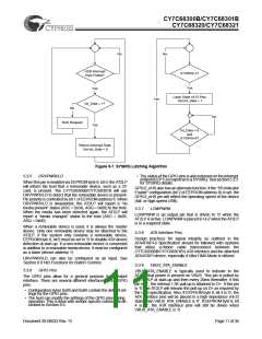
The AT2LP requires a 24-MHz ( 100ppm) signal to derive
internal timing. Typically, a 24-MHz (20-pF, 500-µW, parallel-
24MHz Xtal
12pF
12pF
XTALIN
XTALOUT
Figure 5-6. XTALIN / XTALOUT Diagram
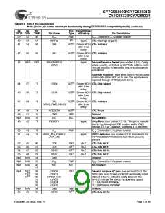
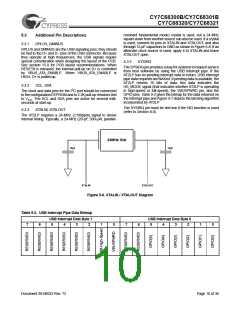
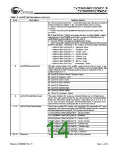
Table 5-2. USB Interrupt Pipe Data Bitmap
USB Interrupt Data Byte 1
USB Interrupt Data Byte 0
7
6
5
4
3
2
1
0
7
6
5
4
3
2
1
0
Document 38-08033 Rev. *D
Page 10 of 36

 CYPRESS [ CYPRESS ]