CY7C64013
CY7C64113
2.0
Functional Overview
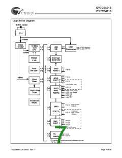
The CY7C64013 and CY7C64113 are 8-bit One Time Programmable microcontrollers that are designed for full-speed USB
applications. The instruction set has been optimized specifically for USB operations, although the microcontrollers can be used
for a variety of non-USB embedded applications.
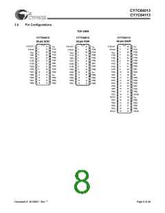
The CY7C64013 features 19 GPIO pins to support USB and other applications. The I/O pins are grouped into three ports (P0[7:0],
P1[7:0], P3[7,2,0]) where each port can be configured as inputs with internal pull-ups, open drain outputs, or traditional CMOS
outputs. There are 16 GPIO pins (Ports 0 and 1) which are rated at 7 mA typical sink current. Port 3 pins are rated at 12 mA
typical sink current, a current sufficient to drive LEDs. Multiple GPIO pins can be connected together to drive a single output for
more drive current capacity. Additionally, each GPIO can be used to generate a GPIO interrupt to the microcontroller. All of the
GPIO interrupts share the same “GPIO” interrupt vector.
Thirty-two GPIO pins (P0[7:0], P1[7:0], P2[7:0], P3[7:0]) and four Digital to Analog Conversion (DAC) pins (P4[7,2:0]) are available
on the CY7C64113. Every DAC pin includes an integrated 14-kΩ pull-up resistor. When a ‘1’ is written to a DAC I/O pin, the output
current sink is disabled and the output pin is driven HIGH by the internal pull-up resistor. When a ‘0’ is written to a DAC I/O pin,
the internal pull-up resistor is disabled and the output pin provides the programmed amount of sink current. A DAC I/O pin can
be used as an input with an internal pull-up by writing a ‘1’ to the pin.
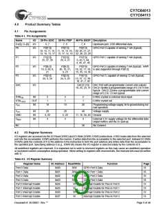
The sink current for each DAC I/O pin can be individually programmed to one of 16 values using dedicated Isink registers. DAC
bits P4[1:0] can be used as high-current outputs with a programmable sink current range of 3.2 to 16 mA (typical). DAC bits
P4[7,2] have a programmable current sink range of 0.2 to 1.0 mA (typical). Multiple DAC pins can be connected together to drive
a single output that requires more sink current capacity. Each I/O pin can be used to generate a DAC interrupt to the microcon-
troller. Also, the interrupt polarity for each DAC I/O pin is individually programmable.
The microcontroller uses an external 6-MHz crystal and an internal oscillator to provide a reference to an internal PLL-based
clock generator. This technology allows the customer application to use an inexpensive 6-MHz fundamental crystal that reduces
the clock-related noise emissions (EMI). A PLL clock generator provides the 6-, 12-, and 48-MHz clock signals for distribution
within the microcontroller.
The CY7C64013 and CY7C64113 have 8 KB of PROM. These parts include power-on reset logic, a watch dog timer, and a 12-bit
free-running timer. The power-on reset (POR) logic detects when power is applied to the device, resets the logic to a known state,
and begins executing instructions at PROM address 0x0000. The watch dog timer is used to ensure the microcontroller recovers
after a period of inactivity. The firmware may become inactive for a variety of reasons, including errors in the code or a hardware
failure such as waiting for an interrupt that never occurs.
The microcontroller can communicate with external electronics through the GPIO pins. An I2C compatible interface accommo-
dates a 100-kHz serial link with an external device. There is also a Hardware Assisted Parallel Interface (HAPI) which can be
used to transfer data to an external device.
The free-running 12-bit timer clocked at 1 MHz provides two interrupt sources, 128-µs and 1.024-ms. The timer can be used to
measure the duration of an event under firmware control by reading the timer at the start of the event and after the event is
complete. The difference between the two readings indicates the duration of the event in microseconds. The upper four bits of
the timer are latched into an internal register when the firmware reads the lower eight bits. A read from the upper four bits actually
reads data from the internal register, instead of the timer. This feature eliminates the need for firmware to try to compensate if
the upper four bits increment immediately after the lower eight bits are read.
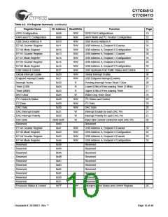
The microcontroller supports 11 maskable interrupts in the vectored interrupt controller. Interrupt sources include the USB Bus
Reset interrupt, the 128-µs (bit 6) and 1.024-ms (bit 9) outputs from the free-running timer, five USB endpoints, the DAC port, the
GPIO ports, and the I2C compatible master mode interface. The timer bits cause an interrupt (if enabled) when the bit toggles
from LOW ‘0’ to HIGH ‘1.’ The USB endpoints interrupt after the USB host has written data to the endpoint FIFO or after the USB
controller sends a packet to the USB host. The DAC ports have an additional level of masking that allows the user to select which
DAC inputs can cause a DAC interrupt. The GPIO ports also have a level of masking to select which GPIO inputs can cause a
GPIO interrupt. For additional flexibility, the input transition polarity that causes an interrupt is programmable for each pin of the
DAC port. Input transition polarity can be programmed for each GPIO port as part of the port configuration. The interrupt polarity
can be rising edge (‘0’ to ‘1’) or falling edge (‘1’ to ‘0’).
Document #: 38-08001 Rev. **
Page 6 of 48

 CYPRESS [ CYPRESS ]