CY7C64013
CY7C64113
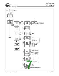
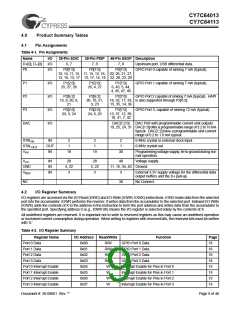
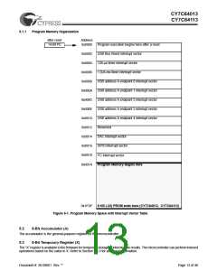
4.0
4.1
Product Summary Tables
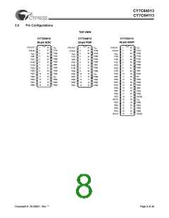
Pin Assignments
Table 4-1. Pin Assignments
Name
I/O
I/O
I/O
28-Pin SOIC
6, 7
28-Pin PDIP
7, 8
48-Pin SSOP Description
D+[0], D–[0]
P0
7, 8
Upstream port, USB differential data.
GPIO Port 0 capable of sinking 7 mA (typical).
P0[7:0]
P0[7:0]
P0[7:0]
10, 14, 11, 15, 11, 15, 12, 16, 20, 26, 21, 27,
12, 16, 13, 17 13, 17, 14, 18 22, 28, 23, 29
P1
I/O
I/O
I/O
I/O
P1[2:0]
25, 27, 26
P1[2:0]
26, 4, 27
P1[7:0]
6, 43, 5, 44,
4, 45, 47, 46
GPIO Port 1 capable of sinking 7 mA (typical).
P2
P2[6:2]
19, 9, 20, 8,
21
P2[6:2]
20, 10, 21,
9, 23
P2[7:0]
GPIO Port 2 capable of sinking 7 mA (typical). HAPI
18, 32, 17, 33, is also supported through P2[6:2].
15, 35, 14, 36
P3
P3[2:0]
23, 5, 24
P3[2:0]
24, 6, 25
P3[7:0]
13, 37, 12, 39,
10, 41, 7, 42
GPIO Port 3, capable of sinking 12 mA (typical).
DAC
DAC[7,2:0]
DAC Port with programmable current sink outputs.
19, 25, 24, 31 DAC[1:0] offer a programmable range of 3.2 to 16 mA
typical. DAC[7,2] have a programmable sink current
range of 0.2 to 1.0 mA typical.
XTALIN
XTALOUT
VPP
IN
OUT
IN
2
1
2
1
2
1
6-MHz crystal or external clock input.
6-MHz crystal out.
18
19
30
Programming voltage supply, tie to ground during nor-
mal operation.
VCC
IN
IN
IN
28
4, 22
3
28
5, 22
3
48
Voltage supply.
GND
VREF
11, 16, 34, 40 Ground.
3
External 3.3V supply voltage for the differential data
output buffers and the D+ pull-up.
NC
38
No Connect.
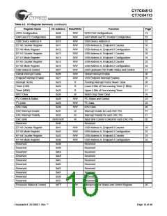
4.2
I/O Register Summary
I/O registers are accessed via the I/O Read (IORD) and I/O Write (IOWR, IOWX) instructions. IORD reads data from the selected
port into the accumulator. IOWR performs the reverse; it writes data from the accumulator to the selected port. Indexed I/O Write
(IOWX) adds the contents of X to the address in the instruction to form the port address and writes data from the accumulator to
the specified port. Specifying address 0 (e.g., IOWX 0h) means the I/O register is selected solely by the contents of X.
All undefined registers are reserved. It is important not to write to reserved registers as this may cause an undefined operation
or increased current consumption during operation. When writing to registers with reserved bits, the reserved bits must be written
with ‘0.’
Table 4-2. I/O Register Summary
Register Name
Port 0 Data
I/O Address Read/Write
Function
Page
18
0x00
0x01
0x02
0x03
0x04
0x05
0x06
0x07
R/W
R/W
R/W
R/W
W
GPIO Port 0 Data
GPIO Port 1 Data
GPIO Port 2 Data
GPIO Port 3 Data
Port 1 Data
18
Port 2 Data
18
Port 3 Data
18
Port 0 Interrupt Enable
Port 1 Interrupt Enable
Port 2 Interrupt Enable
Port 3 Interrupt Enable
Interrupt Enable for Pins in Port 0
Interrupt Enable for Pins in Port 1
Interrupt Enable for Pins in Port 2
Interrupt Enable for Pins in Port 3
19
W
19
W
19
W
19
Document #: 38-08001 Rev. **
Page 9 of 48

 CYPRESS [ CYPRESS ]