CY7C64013
CY7C64113
2
Figure 13-1. I C Data Register 0x29 (separate read/write registers) ............................................. 23
2
Figure 13-2. I C Status and Control Register 0x28 (read/write) .................................................... 23
Figure 15-1. Processor Status and Control Register 0xFF ............................................................ 25
Figure 16-1. Global Interrupt Enable Register 0x20 (read/write) ................................................... 26
Figure 16-2. USB Endpoint Interrupt Enable Register 0x21 (read/write) ...................................... 26
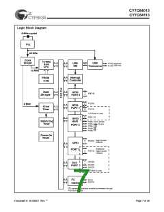
Figure 16-3. Interrupt Controller Functional Diagram .................................................................... 27
Figure 16-4. Interrupt Vector Register 0x23 (read only) .................................................................28
Figure 16-5. GPIO Interrupt Structure .............................................................................................. 29
Figure 17-1. USB Status and Control Register 0x1F (read/write) .................................................. 31
Figure 18-1. USB Device Address Register 0x10 (read/write) ....................................................... 32
Figure 18-2. USB Device Endpoint Zero Mode Register 0x12 (read/write) ................................... 32
Figure 18-3. USB Non-Control Device Endpoint Mode Registers
0x14, 0x16, 0x42, 0x44, (read/write) ............................................................................................... 33
Figure 18-4. USB Endpoint Counter Registers 0x11, 0x13, 0x15, 0x41, 0x43 (read/write) .......... 33
Figure 18-5. Token/Data Packet Flow Diagram ............................................................................... 35
Figure 22-1. Clock Timing ................................................................................................................. 44
Figure 22-2. USB Data Signal Timing ............................................................................................... 44
Figure 22-3. HAPI Read by External Interface from USB Microcontroller .................................... 44
Figure 22-4. HAPI Write by External Device to USB Microcontroller ............................................ 45
LIST OF TABLES
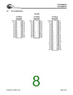
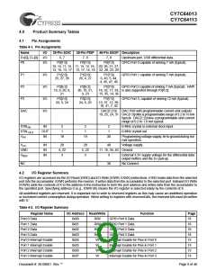
Table 4-1. Pin Assignments ................................................................................................................9
Table 4-2. I/O Register Summary ........................................................................................................9
Table 4-3. Instruction Set Summary .................................................................................................11
Table 9-1. Port Configurations .........................................................................................................18
Table 12-1. HAPI Port Configuration ................................................................................................22
2
Table 12-2. I C Port Configuration ...................................................................................................22
2
Table 13-1. I C Status and Control Register Bit Definitions ..........................................................23
Table 14-1. Port 2 Pin and HAPI Configuration Bit Definitions .....................................................25
Table 16-1. Interrupt Vector Assignments .......................................................................................28
Table 17-1. Control Bit Definition for Upstream Port .....................................................................31
Table 18-1. Memory Allocation for Endpoints ................................................................................32
Table 19-1. USB Register Mode Encoding ......................................................................................36
Table 19-2. Decode table for Table 19-3: “Details of Modes for Differing Traffic Conditions” ...37
Table 19-3. Details of Modes for Differing Traffic Conditions .......................................................38
Document #: 38-08001 Rev. **
Page 4 of 48

 CYPRESS [ CYPRESS ]